 ChipApex | Global Electronic Components Supplier

SEARCH
Search Product
Search Post
— IC芯片 | 连接器 | 传感器 | 被动器件 —
Search productSearch post
— IC芯片 | 连接器 | 传感器 | 被动器件 —
Consult the customer manager about the wholesale price.
consultation hotline:86-132-6715-2157
email:[email protected]
Contact the product manager for consultation. One-stop consultation is available.
Do you want a lower wholesale price? Please send us your inquiry and we will reply immediately.
The BSS205NH6327XTSA1 is an N-channel enhancement mode MOSFET from the OptiMOS 2 series. It features a 20 V drain-source voltage rating and supports a continuous drain current of 2.5 A at 25 °C, with a pulsed capability of 10 A. The device offers a maximum on-state resistance of 85 mΩ at 2.5 V gate drive and 50 mΩ at 4.5 V. It includes avalanche energy ratings (EAS = 10.8 mJ) and high reverse diode dv/dt tolerance (6 kV/µs). Packaged in SOT-23, it operates within a temperature range of -55 °C to 150 °C.
Verify component authenticity by matching the marking code SZS and ordering suffix H6327XTSA1 against official Infineon documentation. Confirm compliance with RoHS directives and halogen-free standards per IEC61249-2-21. Ensure procurement channels provide valid traceability records for AEC-Q101 qualified automotive-grade components.
Select this component when a compact N-channel switch requires operation below standard logic levels. The 2.5 V rated Super Logic level feature allows direct interfacing with low-voltage microcontrollers. Verify that the required thermal management aligns with the specified junction-to-ambient thermal resistance values.
This part belongs to the BSS205N family within Infineon's OptiMOS 2 portfolio. It utilizes silicon technology and is housed in a PG-SOT23 surface-mount package. The product line focuses on optimizing performance for small-signal applications while maintaining automotive reliability standards.
Consult official Infineon cross-reference documentation for verified substitutes. Do not assume functional equivalence based solely on pinout or generic electrical parameters without validating specific dynamic characteristics and package dimensions.
The single pulse avalanche energy (EAS) is rated at 10.8 mJ under conditions of ID=2.5 A and RGS=25 Ω.
Yes, the BSS205NH6327XTSA1 is qualified according to the AEC-Q101 standard.
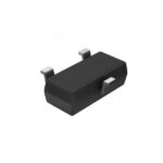 BSS205NH6327XTSA1

The activity of extra discounts on wholesale prices is in full swing…
Please fill in your contact information and we will send you the latest wholesale price list.





