 ChipApex | Global Electronic Components Supplier
SEARCH
Search Product
Search Post
— IC芯片 | 连接器 | 传感器 | 被动器件 —
Search productSearch post
— IC芯片 | 连接器 | 传感器 | 被动器件 —
Consult the customer manager about the wholesale price.
consultation hotline:86-132-6715-2157
email:[email protected]
Contact the product manager for consultation. One-stop consultation is available.
Do you want a lower wholesale price? Please send us your inquiry and we will reply immediately.
The Central Semiconductor BSV79 is an N-channel silicon Junction Field-Effect Transistor (JFET) designed for switching applications. It operates within a drain-source voltage range of 40 V and dissipates up to 350 mW of power. The device features a gate-source reverse voltage rating of 40 V and a maximum junction temperature of +175 °C. Electrical characteristics include a typical on-resistance of 40 Ω at zero gate bias, with a gate-source cutoff voltage ranging from 2.0 V to 7.0 V. The component utilizes a TO-18 metal can package with three leads designated as source, drain, and gate.
Verify the specific ordering suffix required for plating configuration before purchase. The manufacturer offers Tin/Lead or Lead-Free options by appending the corresponding suffix to the part number during the order process. Confirm availability status as the component may be subject to End-of-Life management protocols affecting long-term supply continuity.
Select the BSV79 when an N-channel JFET with a 40 V breakdown voltage and TO-18 mechanical form factor is required. Ensure the circuit design accommodates the specified gate-source cutoff voltage range of 2.0 V to 7.0 V for proper switching thresholds. Verify that the thermal resistance and power dissipation limits align with the system's operating environment and heat sinking capabilities.
The BSV79 belongs to a family of N-channel silicon JFETs manufactured by Central Semiconductor Corp. It shares the same package outline and general switching architecture with the BSV80 model, though electrical parameters such as on-resistance and cutoff voltage differ between the two variants. Both devices utilize the standard TO-18 case style.
Official documentation lists no direct replacement part numbers for the BSV79. The manufacturer indicates that stock only is available for this component. Engineers seeking alternatives must evaluate third-party discrete JFETs based on matching voltage ratings, package dimensions, and electrical performance curves.
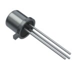 BSV79
BSV79
The activity of extra discounts on wholesale prices is in full swing…
Please fill in your contact information and we will send you the latest wholesale price list.





