 ChipApex | Global Electronic Components Supplier
SEARCH
Search Product
Search Post
— IC芯片 | 连接器 | 传感器 | 被动器件 —
Search productSearch post
— IC芯片 | 连接器 | 传感器 | 被动器件 —
Consult the customer manager about the wholesale price.
consultation hotline:86-132-6715-2157
email:[email protected]
Contact the product manager for consultation. One-stop consultation is available.
Do you want a lower wholesale price? Please send us your inquiry and we will reply immediately.
The BU8255KVT is a 35-bit LVDS receiver and 5:35 deserializer from Rohm Semiconductor, designed for high-speed serial-to-parallel data conversion. It accepts five differential LVDS data channels and one clock channel, converting them into 35 parallel LVCMOS outputs. The device supports clock frequencies from 8MHz to 112MHz, enabling throughput rates up to 784Mbps per channel or 3.92Gbps total at 112MHz. It features user-programmable output triggering on either the rising or falling edge of the clock. The IC includes power-down modes and an internal PLL, packaged in a TQFP64V format with separate power domains for LVDS inputs, digital core, and PLL.
Verify the specific ordering suffix 'E2' against the manufacturer's current catalog to confirm package type and environmental compliance status. Ensure the TQFP64V package variant matches the required PCB footprint and thermal dissipation capabilities for the target application environment.
Select this component when interfacing LVDS serializers like the BU8254KVT to LVCMOS display controllers. Ensure the design accommodates the 3.3V supply voltage and provides adequate decoupling for the LVDD, VDD, and PVDD pins. Verify that the clock source falls within the 8MHz to 112MHz operational range for reliable PLL locking.
This part belongs to Rohm's LVDS interface family, specifically functioning as a deserializer counterpart to serializers like the BU8254KVT. It is engineered for video signal transmission where cable count reduction is critical. The device integrates a PLL for clock recovery and supports multiple standard video resolutions through its parallel output structure.
No public substitute part numbers are documented in the provided datasheet. Designers should verify compatibility with existing serializer components, particularly the recommended BU8254KVT, before considering alternative deserializers.
The R/F pin selects the triggering edge. A High level latches data on the rising edge of the clock, while a Low level latches data on the falling edge.
The RESERVE pin must be held at a Low level for normal operation of the device.
Power on reset is not mandatory but is strongly recommended for internal logic initialization. This can be achieved using a CR circuit or an external specific IC connected to the PD pin.
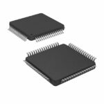 BU8255KVT-E2
The activity of extra discounts on wholesale prices is in full swing…
Please fill in your contact information and we will send you the latest wholesale price list.






