ChipApex | Global Electronic Components Supplier

SEARCH
Search Product
Search Post
— IC芯片 | 连接器 | 传感器 | 被动器件 —
Search productSearch post
— IC芯片 | 连接器 | 传感器 | 被动器件 —
Consult the customer manager about the wholesale price.
consultation hotline:86-132-6715-2157
email:[email protected]
Contact the product manager for consultation. One-stop consultation is available.
Do you want a lower wholesale price? Please send us your inquiry and we will reply immediately.
The BUK626R2-40C is an N-channel TrenchMOS intermediate level enhancement mode Field-Effect Transistor (FET) designed for high-performance automotive applications. It operates with a drain-source voltage of 40 V and supports continuous drain currents up to 90 A at 25 °C mounting base temperature. The device delivers total power dissipation of 128 W under standard conditions, with a maximum on-state resistance of 6.2 mΩ at VGS = 10 V and ID = 15 A. It features a junction temperature rating of 175 °C and complies with the AEC-Q101 standard.
Verify the specific ordering suffix against manufacturer documentation to confirm package type and tape/reel specifications. Confirm that the component meets current RoHS and REACH compliance requirements for your region. Ensure design margins account for the absolute maximum ratings, particularly regarding avalanche energy limits and thermal resistance characteristics during operation.
Select this component when designing circuits requiring robust N-channel switching with intermediate gate drive levels. The DPAK package provides effective thermal management for high-current applications. Consider the 175 °C junction temperature capability for environments where standard components may exceed their thermal limits. Verify compatibility with existing gate driver voltages given the specified threshold voltage range.
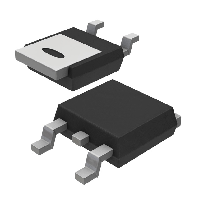
This part belongs to Nexperia's TrenchMOS family of N-channel MOSFETs, utilizing advanced trench technology for low on-resistance and efficient switching. The BUK626R2-40C specifically targets automotive markets, offering durability and performance suitable for harsh operating conditions. It is housed in a SOT428 (DPAK) plastic surface-mounted package, providing a balance between electrical performance and thermal dissipation capabilities.
Consult official Nexperia substitution guides or datasheets for verified equivalent parts. Do not assume pin-compatible replacements without verifying electrical parameters and thermal characteristics against the original specification.
The maximum non-repetitive drain-source avalanche energy is 113 mJ under conditions of ID = 90 A, Vsup ≤ 40 V, RGS = 50 Ω, VGS = 10 V, and initial junction temperature of 25 °C.
The normalized drain-source on-state resistance increases with junction temperature. At 175 °C, the maximum on-state resistance can reach approximately 13 mΩ when tested at VGS = 10 V and ID = 15 A.
 BUK626R2-40C,118

The activity of extra discounts on wholesale prices is in full swing…
Please fill in your contact information and we will send you the latest wholesale price list.