ChipApex | Global Electronic Components Supplier
SEARCH
Search Product
Search Post
— IC芯片 | 连接器 | 传感器 | 被动器件 —
Search productSearch post
— IC芯片 | 连接器 | 传感器 | 被动器件 —
Consult the customer manager about the wholesale price.
consultation hotline:86-132-6715-2157
email:[email protected]
Contact the product manager for consultation. One-stop consultation is available.
Do you want a lower wholesale price? Please send us your inquiry and we will reply immediately.
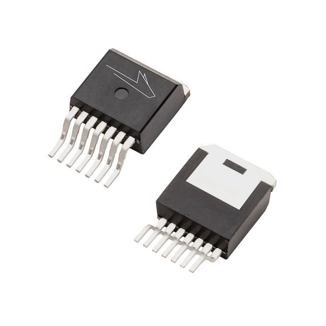
The C3M0021120J2 is a third-generation silicon carbide (SiC) MOSFET from Wolfspeed, designed for high-efficiency power conversion. It features an N-channel enhancement mode configuration housed in a TO-263-7XL package with a separate Kelvin source pin. Key electrical parameters include a drain-source voltage of 1200 V and a maximum continuous drain current of 114 A at 25°C case temperature. The device exhibits a typical on-resistance of 21 mΩ and supports operation up to a junction temperature of 175°C.
Verify the specific ordering suffix J2 corresponds to the required reel packaging format. Confirm that the TO-263-7XL footprint matches the target PCB layout. Ensure the procurement channel provides valid RoHS compliance documentation. Cross-reference the datasheet revision date against manufacturing lot codes to ensure component version consistency.
Select this component when system requirements demand high blocking voltage combined with low conduction losses. The separate Kelvin source pin is critical for applications requiring precise gate drive control to mitigate parasitic inductance effects. Evaluate thermal resistance characteristics against the available heatsinking capacity to ensure junction temperatures remain within the specified operational limits during peak load conditions.
This part belongs to the C3M series of discrete Silicon Carbide MOSFETs manufactured by Wolfspeed. It represents an evolution in wide-bandgap semiconductor technology, offering improved power density compared to previous generations. The device is engineered to replace traditional silicon counterparts in high-voltage industrial and automotive applications.
Direct replacement requires verifying pin compatibility with the TO-263-7XL footprint. Alternative devices must match or exceed the 1200 V rating and comparable on-resistance values. Thermal interface material selection may need adjustment if the alternative package differs slightly in dimensions.
The device includes dedicated power source pins and a separate Kelvin source pin. This configuration isolates the sensitive gate drive circuit from high-current switching noise, reducing gate ringing and improving switching stability.
The intrinsic body diode features fast reverse recovery characteristics with low reverse recovery charge, which helps reduce switching losses during freewheeling operations in bridge configurations.
 C3M0021120J2-TR
The activity of extra discounts on wholesale prices is in full swing…
Please fill in your contact information and we will send you the latest wholesale price list.