ChipApex | Global Electronic Components Supplier
SEARCH
Search Product
Search Post
— IC芯片 | 连接器 | 传感器 | 被动器件 —
Search productSearch post
— IC芯片 | 连接器 | 传感器 | 被动器件 —
Consult the customer manager about the wholesale price.
consultation hotline:86-132-6715-2157
email:[email protected]
Contact the product manager for consultation. One-stop consultation is available.
Do you want a lower wholesale price? Please send us your inquiry and we will reply immediately.
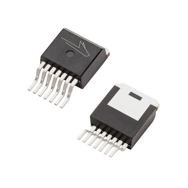
The C3M0045065J1 is a third-generation silicon carbide (SiC) MOSFET from Wolfspeed, packaged in a TO-263-7L XL. It features an N-channel enhancement mode configuration with a 650 V drain-source voltage rating and a maximum gate-source voltage of +19 V. The device exhibits a typical on-resistance of 45 mΩ at 25°C and supports a continuous drain current of 47 A. Key electrical parameters include a total gate charge of 61 nC, input capacitance of 1621 pF, and reverse recovery charge of 206 nC. Thermal characteristics specify a junction-to-case resistance of 0.85 °C/W, with an operating temperature range spanning -40°C to +175°C.
Verify the specific package variant matches the required PCB footprint, as the J1 suffix denotes the TO-263-7L XL form factor. Confirm compliance documentation availability for REACh SVHC status prior to integration. Ensure the ordering part number aligns with the intended manufacturing revision, as datasheet updates may occur without immediate notification. Validate that the selected component meets all applicable safety standards for the target end-use environment.
Select this component when system efficiency requires minimizing both conduction and switching losses in hard-switching topologies. The separate driver source pin facilitates precise control over turn-on transients, reducing electromagnetic interference. Consider the thermal resistance and safe operating area curves for heat sink sizing under varying duty cycles. Evaluate the gate charge requirements against available driver capabilities to optimize switching frequency performance.
This discrete MOSFET belongs to the C3M series of silicon carbide power devices manufactured by Wolfspeed. It represents the company's third-generation technology platform, designed to replace traditional silicon counterparts in high-voltage applications. The product line focuses on enhancing power density and reducing overall system weight through superior material properties and optimized packaging solutions.
Direct cross-references are not explicitly documented in the provided datasheet. Designers should evaluate alternative Wolfspeed models within the same 650 V generation family based on matching RDS(on) and package dimensions. Verify pinout compatibility and thermal characteristics before substituting components in existing layouts.
The package includes dedicated Kelvin source pins (Pin 2) separated from the main power source tabs. This design allows the gate driver to sense the source potential directly at the die, minimizing the impact of stray inductance in the power path and reducing gate voltage ringing during switching transitions.
The intrinsic diode exhibits fast reverse recovery characteristics with a typical reverse recovery charge (Qrr) of 206 nC at 25°C. This low charge minimizes energy loss during the dead-time intervals in bridge configurations, contributing to higher overall system efficiency.
 C3M0045065J1
The activity of extra discounts on wholesale prices is in full swing…
Please fill in your contact information and we will send you the latest wholesale price list.