ChipApex | Global Electronic Components Supplier
SEARCH
Search Product
Search Post
— IC芯片 | 连接器 | 传感器 | 被动器件 —
Search productSearch post
— IC芯片 | 连接器 | 传感器 | 被动器件 —
Consult the customer manager about the wholesale price.
consultation hotline:86-132-6715-2157
email:[email protected]
Contact the product manager for consultation. One-stop consultation is available.
Do you want a lower wholesale price? Please send us your inquiry and we will reply immediately.
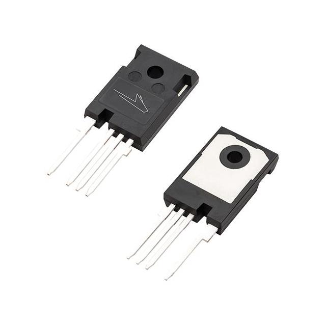
The C3M0075120K is a third-generation Silicon Carbide (SiC) MOSFET from Wolfspeed, designed for high-voltage power switching applications. It features an N-channel enhancement mode configuration housed in a TO-247-4 package with a separate driver source pin to minimize gate ringing. The device offers a drain-source voltage of 1200V and a typical on-resistance of 75mΩ at 25°C. Key electrical parameters include a continuous drain current of 31A, a maximum power dissipation of 114W, and an operating junction temperature range from -55°C to +150°C. The component supports high-speed switching with low capacitances and includes a fast intrinsic diode with low reverse recovery characteristics.
Verify the specific ordering suffix and package marking against the official Wolfspeed datasheet to ensure correct part identification. Confirm RoHS compliance and REACH SVHC status requirements prior to integration. Ensure that the procurement channel provides valid traceability documentation. Check for any recent revision history updates that may affect thermal or electrical specifications. Validate that the supplier can provide the necessary technical support documents such as SPICE models.
Select this component for designs requiring high efficiency and power density in high-voltage environments. The separate driver source pin is critical for minimizing parasitic inductance effects in high-frequency switching circuits. Consider the thermal resistance and derating curves when designing heat sinks for continuous operation. Evaluate the gate charge requirements against available driver capabilities to optimize switching performance. Ensure the application voltage and current ratings remain within the specified safe operating area limits.
This device belongs to Wolfspeed's third-generation Silicon Carbide MOSFET portfolio, which focuses on improving system efficiency through reduced switching and conduction losses. The TO-247-4 package is a standard industry form factor facilitating through-hole mounting. The product line is engineered to support higher switching frequencies, allowing for smaller passive components in power conversion topologies. It represents an advancement over previous generations by offering improved ruggedness and thermal performance.
Direct replacement requires verifying pin compatibility and electrical parameter equivalence. Compare on-resistance, breakdown voltage, and thermal resistance values carefully. Ensure the substitute device supports the required gate drive voltage levels and switching speeds. Review the package dimensions to confirm mechanical fit within the existing PCB layout and heatsink interface.
The separate driver source pin (Pin 3) isolates the high-current power source path from the sensitive gate drive return path. This design minimizes ground bounce and reduces gate ringing during high-speed switching transitions.
The intrinsic body diode exhibits low reverse recovery charge (Qrr), which reduces switching losses during hard-switching operations. It is characterized by a peak reverse recovery current and short reverse recovery time, enhancing efficiency in synchronous rectification applications.
The recommended turn-on gate voltage is 15V with a ±5% regulation tolerance. The maximum transient gate-source voltage is +19V, while the static operational range extends down to -4V for turn-off.
 C3M0075120K
The activity of extra discounts on wholesale prices is in full swing…
Please fill in your contact information and we will send you the latest wholesale price list.