ChipApex | Global Electronic Components Supplier
SEARCH
Search Product
Search Post
— IC芯片 | 连接器 | 传感器 | 被动器件 —
Search productSearch post
— IC芯片 | 连接器 | 传感器 | 被动器件 —
Consult the customer manager about the wholesale price.
consultation hotline:86-132-6715-2157
email:[email protected]
Contact the product manager for consultation. One-stop consultation is available.
Do you want a lower wholesale price? Please send us your inquiry and we will reply immediately.
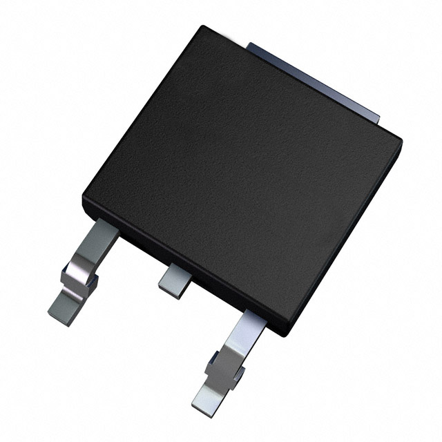
The Comchip Technology CDBD660-G is a Chip Schottky Barrier Rectifier housed in a TO-252/DPAK surface-mount package. It features a repetitive peak reverse voltage of 60 V and a continuous forward rectified current of 6.0 A at 25°C. The device exhibits a maximum forward voltage drop of 0.75 V at the rated current and supports a maximum non-repetitive forward surge current of 80 A for an 8.3 ms half-sine wave. Thermal resistance from junction to case is 1.9 °C/W, with a junction-to-ambient resistance of 56 °C/W. Operating temperatures range from -55°C to +150°C.
Verify the specific ordering suffix matches the required voltage rating within the CDBD6 series. Confirm compliance with MIL-STD-19500/228 environmental standards if applicable. Ensure the TO-252/DPAK footprint aligns with the suggested pad layout provided in the datasheet. Check for RoHS compliance status prior to final procurement authorization.
Select this component when a 60 V reverse voltage rating and 6.0 A continuous current capability are required in a DPAK package. Consider the 0.75 V forward voltage drop for efficiency calculations. Evaluate the thermal resistance values against the expected ambient temperature and derating curves to ensure safe junction temperature operation under load conditions.
This part belongs to the CDBD6 series of Chip Schottky Barrier Rectifiers manufactured by Comchip Technology. The series covers reverse voltages from 20 V to 100 V, all sharing the same 6.0 A forward current rating and TO-252/DPAK mechanical outline. The CDBD660-G specifically addresses the 60 V segment of this standardized product line.
Direct substitutes include other 60 V, 6 A Schottky rectifiers in the TO-252/DPAK package. Verify pinout compatibility and thermal characteristics before substitution.
The maximum operating junction temperature is +150°C.
Polarity is indicated by the cathode band marked on the device casing.
 CDBD660-G
The activity of extra discounts on wholesale prices is in full swing…
Please fill in your contact information and we will send you the latest wholesale price list.