 ChipApex | Global Electronic Components Supplier
CDC2509APWR
Search Product
Search Post
— IC芯片 | 连接器 | 传感器 | 被动器件 —
Search productSearch post
— IC芯片 | 连接器 | 传感器 | 被动器件 —
Consult the customer manager about the wholesale price.
consultation hotline:86-132-6715-2157
email:[email protected]
Contact the product manager for consultation. One-stop consultation is available.
Do you want a lower wholesale price? Please send us your inquiry and we will reply immediately.
The CDC2509APWR is a 3.3-V phase-lock loop (PLL) clock driver manufactured by Texas Instruments in a 24-pin TSSOP package. It operates within a supply voltage range of 3 V to 3.6 V and supports frequencies up to 100 MHz. The device distributes one clock input to nine outputs, organized into two banks: five outputs (1Y0-1Y4) and four outputs (2Y0-2Y3). Each output includes an integrated 25-Ω series-damping resistor. The unit functions across an operating temperature range of 0°C to 70°C.
Verify the specific revision status of the SCAS603B datasheet before implementation, as the document indicates a July 2001 revision. Confirm that the application environment remains within the specified 0°C to 70°C operating temperature range. Ensure AVCC is properly decoupled and that the stabilization time requirement of 1 ms is accommodated during power-up sequences to achieve valid phase lock.
Select this component when a low-skew, low-jitter clock distribution solution is required for synchronous memory systems. The integrated damping resistors simplify board layout by removing the need for external components. Consider the 1 ms stabilization time necessary for PLL locking when designing system power sequencing. Verify that the 100 MHz maximum frequency meets the target system timing requirements.
This part belongs to the CDC2509 family of 3.3-V PLL clock drivers from Texas Instruments. Variants such as the CDC2509C offer similar functionality but may differ in electrical specifications or qualification standards. The 'A' suffix typically denotes specific performance grades or manufacturing lots within the standard product line.
The CDC2509CPWR is a documented alternative within the same family offering identical 1-to-9 PLL clock driver functionality in a 24-TSSOP package.
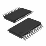 CDC2509APWR
The activity of extra discounts on wholesale prices is in full swing…
Please fill in your contact information and we will send you the latest wholesale price list.





