 ChipApex | Global Electronic Components Supplier
CDC2509BPWR
Search Product
Search Post
— IC芯片 | 连接器 | 传感器 | 被动器件 —
Search productSearch post
— IC芯片 | 连接器 | 传感器 | 被动器件 —
Consult the customer manager about the wholesale price.
consultation hotline:86-132-6715-2157
email:[email protected]
Contact the product manager for consultation. One-stop consultation is available.
Do you want a lower wholesale price? Please send us your inquiry and we will reply immediately.
The CDC2509BPWR is a 3.3-V phase-locked loop (PLL) clock driver manufactured by Texas Instruments. It features one differential input and nine true outputs, designed for high-speed clock distribution in memory systems. The device operates within a supply voltage range of 3.0 V to 3.6 V and supports maximum output frequencies up to 140 MHz. It is housed in a 24-pin TSSOP package with an exposed pad for thermal management. The component functions as a clock buffer and driver, utilizing PLL technology to manage signal integrity and timing requirements for DRAM DIMM applications.
Verify the specific suffix 'PWR' indicates the tape-and-reel packaging format when sourcing components. Confirm that the device meets RoHS compliance standards required for your assembly process. Ensure the supplier provides traceability documentation consistent with Texas Instruments manufacturing records. Check for any obsolescence notices or last-time-buy alerts associated with this specific part number variant before finalizing procurement plans.
Select this component when a single differential input must drive nine distinct clock loads in a 3.3-V environment. Compare against the CDCF2509 series if non-PLL buffered outputs are sufficient for the application. Consider the TSSOP-24 package constraints regarding thermal dissipation and PCB layout space. Verify that the 140 MHz maximum frequency aligns with the target memory speed requirements.
This part belongs to the CDC2509B family of 3.3-V PLL clock drivers from Texas Instruments. It shares functional similarities with the CDC2509C and CDC2510 series but differs in output count and specific electrical characteristics. The device is engineered to replace older generation clock buffers in modern memory designs requiring lower power consumption and improved jitter performance.
Publicly confirmed substitute part numbers include CDC2509BPW and CDC2509BPWG4. These variants share identical electrical specifications and pinouts, differing primarily in packaging type or lead-free status. Verify compatibility with existing board layouts before substitution.
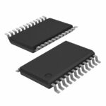 CDC2509BPWR
The activity of extra discounts on wholesale prices is in full swing…
Please fill in your contact information and we will send you the latest wholesale price list.






