 ChipApex | Global Electronic Components Supplier
CDC2582PAH
Search Product
Search Post
— IC芯片 | 连接器 | 传感器 | 被动器件 —
Search productSearch post
— IC芯片 | 连接器 | 传感器 | 被动器件 —
Consult the customer manager about the wholesale price.
consultation hotline:86-132-6715-2157
email:[email protected]
Contact the product manager for consultation. One-stop consultation is available.
Do you want a lower wholesale price? Please send us your inquiry and we will reply immediately.
The CDC2582PAH is a 3.3-V phase-locked loop clock driver featuring differential LVPECL inputs and twelve TTL-compatible outputs in a 52-pin Quad Flatpack package. It operates at frequencies from 50 MHz to 100 MHz, or down to 25 MHz for half-frequency configurations. The device includes an integrated PLL with no external RC network required, internal 26-ohm series resistors for signal integrity, and distributed VCC/GND pins to reduce switching noise. Outputs are configurable via SEL1 and SEL0 to operate at one-half, same, or double the input frequency.
Verify the specific ordering suffix PAH corresponds to the 52-pin Quad Flatpack package configuration. Confirm that the component meets RoHS compliance standards as indicated in the datasheet documentation. Ensure the supply voltage matches the recommended 3.3-V operating range before integration into the design.
Select this component when a low-jitter, low-skew clock driver is required for 3.3-V systems. It is suitable for applications needing frequency multiplication or division relative to a differential LVPECL source. Consider the stabilization time requirements for the internal PLL when designing the power-up sequence.
This device belongs to Texas Instruments' EPIC-IIB BiCMOS family, designed for high performance and reduced power dissipation. It serves as a specialized clock driver solution for systems requiring precise phase alignment between differential inputs and multiple TTL-compatible outputs.
No direct public substitute part numbers are documented in the provided datasheet. Verify compatibility with existing PCB footprints and electrical specifications if considering alternative clock drivers.
No, the CDC2582 does not require an external RC network; the loop filter is included on-chip to minimize component count and board space.
One of the twelve Y outputs must be externally wired to the FBIN pin to provide the feedback signal for frequency and phase lock.
The TEST pin bypasses the PLL circuitry for factory testing. For normal operation, it should be strapped to GND.
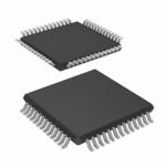 CDC2582PAH
The activity of extra discounts on wholesale prices is in full swing…
Please fill in your contact information and we will send you the latest wholesale price list.






