 ChipApex | Global Electronic Components Supplier
CDC536DBRG4
Search Product
Search Post
— IC芯片 | 连接器 | 传感器 | 被动器件 —
Search productSearch post
— IC芯片 | 连接器 | 传感器 | 被动器件 —
Consult the customer manager about the wholesale price.
consultation hotline:86-132-6715-2157
email:[email protected]
Contact the product manager for consultation. One-stop consultation is available.
Do you want a lower wholesale price? Please send us your inquiry and we will reply immediately.
The CDC536DBRG4 is a PLL clock driver manufactured by Texas Instruments, designed for frequency synthesis and distribution. It operates within a supply voltage range of 3V to 3.6V and supports a maximum frequency of 100MHz. The device features a single circuit with a 1:6 input-to-output ratio, utilizing TTL inputs and LVTTL outputs. It includes integrated divider and multiplier capabilities, housed in a 28-SSOP package measuring 0.209 inches (5.30mm) in width. The component functions reliably across an operating temperature range of 0°C to 70°C.
Verify the specific suffix 'G4' against current manufacturer documentation to confirm RoHS compliance status and lead-free material composition. Confirm that the 28-SSOP package dimensions match the design footprint requirements. Check for any recent lifecycle notices or obsolescence warnings directly from Texas Instruments before finalizing procurement plans.
Select this component when a single-input, six-output clock driver with internal frequency control is required. Ensure the system power supply remains strictly between 3V and 3.6V to maintain operational integrity. Verify that the 0°C to 70°C commercial temperature range meets the environmental constraints of the target application board.
This part belongs to the CDC536 family of PLL clock drivers from Texas Instruments. It shares core functional specifications with variants such as CDC536DBG4 and CDC536DB, differing primarily in packaging or manufacturing lot details. The device serves as a specialized solution for generating multiple synchronized clock signals from a single reference input.
The CDC536DB is listed as a manufacturer-recommended alternative. Verify pin compatibility and electrical parameter equivalence before substitution.
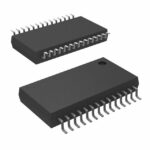 CDC536DBRG4
The activity of extra discounts on wholesale prices is in full swing…
Please fill in your contact information and we will send you the latest wholesale price list.





