 ChipApex | Global Electronic Components Supplier

SEARCH
Search Product
Search Post
— IC芯片 | 连接器 | 传感器 | 被动器件 —
Search productSearch post
— IC芯片 | 连接器 | 传感器 | 被动器件 —
Consult the customer manager about the wholesale price.
consultation hotline:86-132-6715-2157
email:[email protected]
Contact the product manager for consultation. One-stop consultation is available.
Do you want a lower wholesale price? Please send us your inquiry and we will reply immediately.
The CDCDB800RSLT is an 8-output LP-HCSL clock buffer compliant with the DB800ZL specification, designed for PCIe Gen 1 through Gen 7 reference clock distribution. It operates on a single 3V to 3.6V supply and supports input frequencies up to 250 MHz. The device features a maximum propagation delay of 3 ns and output-to-output skew under 50 ps. Additive phase jitter ranges from 11.3 fs RMS (PCIe Gen 7 filter) to 38 fs RMS (DB2000Q filter). It includes programmable 85Ω or 100Ω differential terminations, individual hardware output enables, and SMBus control within a 48-pin VQFN package.
Verify the ordering suffix 'RSL' corresponds to the Tape & Reel packaging format as specified in the datasheet orderable addendum. Confirm that the specific revision level matches the required system documentation updates. Ensure compatibility with the 48-VQFN (6x6mm) footprint during PCB layout verification.
Select this component when distributing reference clocks for high-speed serial interfaces requiring DB800ZL compliance. The device supports both Common Clock and Individual Reference architectures. Verify that the system board impedance aligns with the programmable 85Ω or 100Ω termination settings to ensure signal integrity.
The CDCDB800RSLT belongs to the CDCDB800 family of clock buffers manufactured by Texas Instruments. It serves as a derivative buffer meeting or exceeding the DB800ZL and DB2000Q specifications. The 'RSL' suffix denotes the specific tape and reel packaging variant of the 48-pin VQFN package.
The CDCDB800RSLR is a compatible alternative within the same family, differing primarily in its packaging configuration rather than functional electrical parameters.
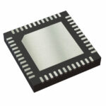 CDCDB800RSLT

The activity of extra discounts on wholesale prices is in full swing…
Please fill in your contact information and we will send you the latest wholesale price list.





