 ChipApex | Global Electronic Components Supplier

SEARCH
Search Product
Search Post
— IC芯片 | 连接器 | 传感器 | 被动器件 —
Search productSearch post
— IC芯片 | 连接器 | 传感器 | 被动器件 —
Consult the customer manager about the wholesale price.
consultation hotline:86-132-6715-2157
email:[email protected]
Contact the product manager for consultation. One-stop consultation is available.
Do you want a lower wholesale price? Please send us your inquiry and we will reply immediately.
The CDCLVP111HFG/EM is a low-voltage, 1:10 LVPECL clock driver with selectable inputs, designed for high-speed clock distribution. It accepts differential LVPECL, LVECL, LVDS, CML, or SSTL inputs and distributes them to ten differential LVPECL outputs. The device supports a supply voltage range of 2.375 V to 3.8 V and operates from -55°C to 125°C. Key electrical parameters include a maximum frequency of 3.5 GHz, typical output skew of 15 ps, additive jitter less than 1 ps, and propagation delay under 355 ps. It is housed in a 36-pin Ceramic Flat Pack (CFP) package.
Verify that the /EM suffix indicates engineering evaluation samples intended for evaluation only. These units are processed to a non-compliant flow without burn-in and are tested at 25°C only. They are not suitable for qualification, production, radiation testing, or flight use, and do not carry performance warranties over the full MIL specified temperature range.
Select this component for applications requiring low-additive jitter (<1 ps) and low-output skew (typical 15 ps) in harsh environments. Ensure the design accommodates the 36-pin CFP package dimensions. Verify power supply decoupling requirements, as the device is sensitive to noise on the power supply which can increase additive jitter.
This part belongs to the CDCLVP111-SP family, which is characterized for extended temperature ranges and offers product traceability. The HFG suffix denotes the 36-pin Ceramic Flat Pack package. The /EM suffix specifically identifies the unit as an engineering evaluation sample, distinct from standard production units.
Standard production equivalents include CDCLVP111SPHFG. For non-military applications, consider CDCLVP111VFR or CDCLVP111MVFREP, noting differences in operating temperature range and packaging.
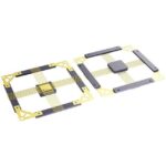 CDCLVP111HFG/EM

The activity of extra discounts on wholesale prices is in full swing…
Please fill in your contact information and we will send you the latest wholesale price list.






