ChipApex | Global Electronic Components Supplier
SEARCH
Search Product
Search Post
— IC芯片 | 连接器 | 传感器 | 被动器件 —
Search productSearch post
— IC芯片 | 连接器 | 传感器 | 被动器件 —
Consult the customer manager about the wholesale price.
consultation hotline:86-132-6715-2157
email:[email protected]
Contact the product manager for consultation. One-stop consultation is available.
Do you want a lower wholesale price? Please send us your inquiry and we will reply immediately.
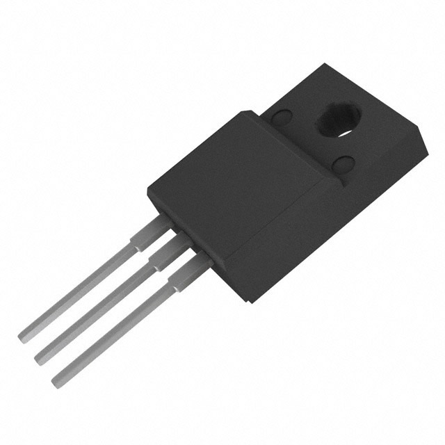
The CDMSJ22013.8-650 is an N-channel Super Junction MOSFET rated for 650V drain-source voltage and 13.8A continuous drain current at 25°C. It features a maximum on-resistance of 280mΩ at VGS=10V and ID=4.4A, with a gate charge of 30nC. The device operates within a junction temperature range of -55°C to +150°C and is housed in a TO-220FP package.
Verify the specific ordering suffix against manufacturer documentation to confirm plating options, such as Tin/Lead or Lead-Free finishes. Ensure the requested part number matches the exact electrical ratings and package type required for the design. Cross-reference datasheet revisions to confirm parameter consistency before finalizing procurement specifications.
Select this component for high-voltage applications requiring low conduction losses and rapid switching speeds. The Super Junction technology provides an optimal balance between RDS(on) and gate charge. Consider thermal management requirements, as continuous current drops significantly at elevated case temperatures compared to room temperature ratings.
This device belongs to Central Semiconductor's Super Junction MOSFET family, designed specifically for high-efficiency power conversion. It utilizes advanced semiconductor architecture to achieve superior performance metrics compared to traditional planar MOSFETs in similar voltage classes.
Consult official substitution guides for verified equivalents. Do not assume pin compatibility or electrical equivalence with other 650V MOSFETs without verifying datasheet parameters.
The maximum operating and storage junction temperature is +150°C.
At a case temperature of 100°C, the continuous drain current is derated to 8.7A from the 13.8A rating at 25°C.
 CDMSJ22013.8-650 SL
The activity of extra discounts on wholesale prices is in full swing…
Please fill in your contact information and we will send you the latest wholesale price list.