ChipApex | Global Electronic Components Supplier
SEARCH
Search Product
Search Post
— IC芯片 | 连接器 | 传感器 | 被动器件 —
Search productSearch post
— IC芯片 | 连接器 | 传感器 | 被动器件 —
Consult the customer manager about the wholesale price.
consultation hotline:86-132-6715-2157
email:[email protected]
Contact the product manager for consultation. One-stop consultation is available.
Do you want a lower wholesale price? Please send us your inquiry and we will reply immediately.
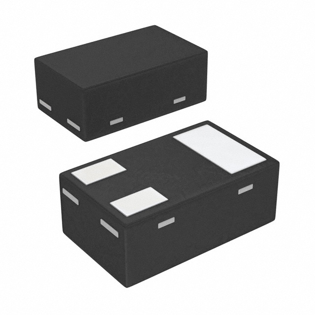
The CEDM7004 TR PBFREE is a surface-mount N-channel enhancement-mode MOSFET manufactured by Central Semiconductor Corp. It utilizes an N-Channel DMOS process designed for high-speed pulsed amplifier and driver applications. The device features a low profile SOT-883L package with a maximum height of 0.40 mm. Key electrical parameters include a drain-source voltage rating of 30 V, a continuous drain current of 1.78 A at 25°C case temperature, and a power dissipation capacity of 100 mW. The component operates within a junction temperature range of -65 to +150 °C.
Verify the specific ordering suffix when purchasing. The 'PBFREE' designation indicates lead-free plating options as defined by manufacturer standards. Confirm the exact package variant, such as SOT-883L or SOT-883VL, if dimensional constraints are critical. Ensure compatibility with RoHS regulations if required by the end application. Cross-reference datasheet revision dates during procurement to ensure accurate parameter data.
Select this component for designs requiring compact surface-mount solutions with low threshold voltage capabilities. The logic-level compatibility allows direct interfacing with standard digital control signals. Evaluate thermal management requirements carefully due to the 100 mW power dissipation limit in the small form factor. Consider the complementary P-channel device, CEDM8004, for bridge or push-pull configurations.
This part belongs to the CEDM series of surface-mount silicon N-channel enhancement-mode MOSFETs from Central Semiconductor Corp. The series is engineered using an N-Channel DMOS process optimized for high-speed switching performance. The CEDM7004 specifically targets applications demanding low profile packaging and efficient power handling within minimal board space constraints.
The official complementary P-channel substitute is the CEDM8004. Verify pinout compatibility and electrical ratings against existing circuit requirements before substituting with components from other manufacturers.
The maximum continuous gate-source voltage (V GS) is rated at 8.0 V.
Yes, the datasheet explicitly lists logic level compatibility as a feature, supported by a low threshold voltage specification.
The typical total gate charge (Qg) is 0.792 nC under test conditions of V DS=15V, VGS=4.5V, and ID=1.0A.
 CEDM7004 TR PBFREE
The activity of extra discounts on wholesale prices is in full swing…
Please fill in your contact information and we will send you the latest wholesale price list.