 ChipApex | Global Electronic Components Supplier
SEARCH
Search Product
Search Post
— IC芯片 | 连接器 | 传感器 | 被动器件 —
Search productSearch post
— IC芯片 | 连接器 | 传感器 | 被动器件 —
Consult the customer manager about the wholesale price.
consultation hotline:86-132-6715-2157
email:[email protected]
Contact the product manager for consultation. One-stop consultation is available.
Do you want a lower wholesale price? Please send us your inquiry and we will reply immediately.
The CMKT2222A TR PBFREE is a surface-mount dual NPN small-signal silicon switching transistor manufactured by Central Semiconductor Corp. It consists of two individually isolated transistors in an SOT-363 package, designed for general-purpose and switching applications. Key electrical parameters include a collector-base voltage (V_CBO) of 75 V, collector-emitter voltage (V_CEO) of 40 V, and continuous collector current (I_C) of 600 mA per device. The maximum power dissipation is 350 mW with a thermal resistance (Θ_JA) of 357 °C/W. The transition frequency (f_T) reaches 300 MHz, and the DC current gain (h_FE) ranges from 100 to 300 at I_C = 150 mA.
Verify the specific ordering suffix when purchasing components. The manufacturer specifies that adding the suffix "PBFREE" indicates lead-free plating, while "TIN/LEAD" denotes tin/lead plating options. Confirm the exact part number matches the required plating specification to ensure compliance with project material constraints and environmental regulations.
Select this component for designs requiring two matched or independent NPN transistors in a minimal footprint. The SOT-363 package offers space efficiency compared to discrete single transistors. Ensure the application operates within the 40 V collector-emitter voltage limit and 600 mA continuous current rating per transistor to maintain reliability and performance specifications.
This component belongs to the Central Semiconductor ULTRAmini™ series of surface-mount devices. It utilizes the standard 2222A NPN silicon transistor architecture adapted into a dual configuration. The device is manufactured using an epitaxial planar process and is epoxy molded for robust surface-mount assembly compatibility.
Direct pin-compatible replacements may include other dual NPN transistors in the SOT-363 package, such as the CMXT2222A. Verify that substitute parts meet or exceed the 40 V V_CEO, 600 mA I_C, and 350 mW P_D requirements before implementation.
The marking code on the device is K22.
Pin 1 is Emitter Q1, Pin 2 is Base Q1, Pin 3 is Collector Q2, Pin 4 is Emitter Q2, Pin 5 is Base Q2, and Pin 6 is Collector Q1.
The maximum operating and storage junction temperature is +150 °C.
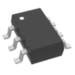 CMKT2222A TR PBFREE
The activity of extra discounts on wholesale prices is in full swing…
Please fill in your contact information and we will send you the latest wholesale price list.






