 ChipApex | Global Electronic Components Supplier
SEARCH
Search Product
Search Post
— IC芯片 | 连接器 | 传感器 | 被动器件 —
Search productSearch post
— IC芯片 | 连接器 | 传感器 | 被动器件 —
Consult the customer manager about the wholesale price.
consultation hotline:86-132-6715-2157
email:[email protected]
Contact the product manager for consultation. One-stop consultation is available.
Do you want a lower wholesale price? Please send us your inquiry and we will reply immediately.
The CPH5905G-TL-E is a composite semiconductor device integrating an N-Channel JFET and an NPN Bipolar Transistor within a single CPH5 package. The JFET section provides a drain-to-source voltage of 15 V, with a drain current (IDSS) ranging from 10.0 to 20.0 mA. The NPN transistor supports a collector-to-emitter voltage of 50 V and a maximum collector current of 150 mA. Total power dissipation is rated at 500 mW on a ceramic board. The device features shared drain and emitter terminals, facilitating efficient mounting.
Verify the specific IDSS rank required for the design, as the G suffix denotes a 10.0 to 20.0 mA range. Confirm that the CPH5 package dimensions and pinout match the PCB land pattern. Ensure thermal management accounts for the 500 mW total power dissipation limit under actual operating conditions rather than ideal test board specifications.
Select this component when space constraints require combining a JFET input stage with a BJT output stage. The shared emitter/drain connection simplifies circuit topology compared to discrete solutions. Consider the H variant if a higher IDSS range of 16.0 to 32.0 mA is necessary for the application requirements.
This part belongs to the CPH5905 family manufactured by onsemi. It utilizes the CPH5 package, which corresponds to SC-74A or SOT-25 form factors. The device replaces older discrete combinations, offering a compact solution for mixed-signal or high-frequency analog applications requiring both field-effect and bipolar transistor characteristics.
CPH5905H-TL-E
The primary difference is the Drain Current (IDSS) classification. The G suffix indicates an IDSS range of 10.0 to 20.0 mA, while the H suffix indicates a range of 16.0 to 32.0 mA.
Pin 1 is Collector, Pin 2 is Gate, Pin 3 is Source, Pin 4 is Emitter/Drain (shared), and Pin 5 is Base.
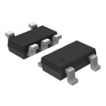 CPH5905G-TL-E
The activity of extra discounts on wholesale prices is in full swing…
Please fill in your contact information and we will send you the latest wholesale price list.





