ChipApex | Global Electronic Components Supplier
SEARCH
Search Product
Search Post
— IC芯片 | 连接器 | 传感器 | 被动器件 —
Search productSearch post
— IC芯片 | 连接器 | 传感器 | 被动器件 —
Consult the customer manager about the wholesale price.
consultation hotline:86-132-6715-2157
email:[email protected]
Contact the product manager for consultation. One-stop consultation is available.
Do you want a lower wholesale price? Please send us your inquiry and we will reply immediately.
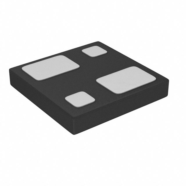
The CSD85302L is a dual N-channel power MOSFET from Texas Instruments, utilizing NexFET technology. It features a PICOSTAR-4 surface-mount package and operates with a drain-source voltage of 20 V. The device supports a continuous drain current of 7 A and maintains a low on-resistance of 24 mΩ. Gate-source voltage limits are ±10 V, with a threshold voltage of 680 mV. Total gate charge is 6 nC, contributing to fast switching characteristics with rise and fall times of 54 ns and 99 ns respectively. Power dissipation is rated at 1.7 W, and the component functions within an operating temperature range of -55°C to +150°C.
Verify the specific ordering suffix when sourcing components, as variations such as LT or standard reel formats may exist. Confirm RoHS compliance status directly from the manufacturer's documentation prior to integration. Ensure that the received parts match the exact part number designation to avoid discrepancies in electrical specifications or package dimensions during assembly.
Select this component for designs requiring a 20 V rating with dual channel capability in a minimal footprint. The 24 mΩ on-resistance is suitable for moderate current loads up to 7 A. Consider the PICOSTAR-4 package constraints for PCB layout and thermal relief requirements. Evaluate the 6 nC gate charge against driver capabilities to ensure adequate switching speed without excessive drive current demands.
This device belongs to the CSD85302L series of NexFET power MOSFETs. It is manufactured by Texas Instruments and represents a silicon-based solution for low-voltage power switching. The product line focuses on integrating multiple channels to reduce board space while maintaining high efficiency in power conversion systems.
Publicly confirmed substitute part numbers are not available in the provided documentation. Cross-referencing requires matching the 20 V, 7 A, dual N-channel specifications and PICOSTAR-4 package dimensions with alternative manufacturers' offerings.
The absolute maximum gate-source voltage is limited to ±10 V.
As a dual N-channel MOSFET, it inherently contains intrinsic body diodes between the source and drain terminals for each channel.
The gate-source threshold voltage is specified at 680 mV under standard test conditions.
 CSD85302L
The activity of extra discounts on wholesale prices is in full swing…
Please fill in your contact information and we will send you the latest wholesale price list.