 ChipApex | Global Electronic Components Supplier

SEARCH
Search Product
Search Post
— IC芯片 | 连接器 | 传感器 | 被动器件 —
Search productSearch post
— IC芯片 | 连接器 | 传感器 | 被动器件 —
Consult the customer manager about the wholesale price.
consultation hotline:86-132-6715-2157
email:[email protected]
Contact the product manager for consultation. One-stop consultation is available.
Do you want a lower wholesale price? Please send us your inquiry and we will reply immediately.
CY2308SXC-5HT is listed in the Clock Generators, PLLs, Frequency Synthesizers range at ChipApex. The manufacturer field lists Infineon Technologies. Its product description is IC FANOUT BUFFER 16SOIC. Review the specifications below when checking this part for your BOM.
The CY2308SXC-5HT is a 3.3V Zero Delay Buffer manufactured by Infineon Technologies, available in a 16-pin 150 mil SOIC package with tape and reel commercial packaging. It operates within a frequency range of 10 MHz to 133.3 MHz. The device features two banks of four outputs each, providing reference divided by two frequencies on both banks. Electrical specifications include a typical cycle-to-cycle jitter of 75 ps at 66.67 MHz with a 15 pF load. Supply voltage ranges from 3.0 V to 3.6 V, with an operating temperature range of 0°C to 70°C for the commercial variant.
Verify the specific ordering suffix HT indicates tape and reel packaging for the SXC commercial grade variant. Confirm that the CY2308SXC-5HT designation aligns with the required Reference/2 output configuration for both output banks as defined in the official Cypress Semiconductor documentation.
Select this component when a zero delay buffer with divided-by-two outputs on all eight pins is required. Ensure the application operates within the 10 MHz to 133.3 MHz frequency range and requires 3.3V operation. Verify that the 16-pin SOIC package meets the board layout constraints and that the commercial temperature range satisfies the environmental requirements.
This part belongs to the CY2308 series of 3.3V Zero Delay Buffers. The -5H suffix denotes a high-drive version configured to provide reference divided by two frequencies on both output banks. The SXC prefix identifies it as a commercial grade device in a standard SOIC package, while the HT suffix specifies tape and reel packaging.
CY2308SXI-5HT (Industrial grade, same package)
The CY2308SXC-5HT provides Reference divided by two frequencies on both Bank A and Bank B outputs.
The input-output propagation delay is adjustable by varying the capacitive load on the FBK (feedback) input pin relative to the other outputs.
The maximum operating frequency is 133.3 MHz for the -1H and -5H devices.
Explore related parts through Clock/Timing, Integrated Circuits (ICs), all product categories, ChipApex homepage.
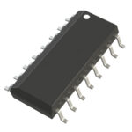 CY2308SXC-5HT

The activity of extra discounts on wholesale prices is in full swing…
Please fill in your contact information and we will send you the latest wholesale price list.





