 ChipApex | Global Electronic Components Supplier

SEARCH
Search Product
Search Post
— IC芯片 | 连接器 | 传感器 | 被动器件 —
Search productSearch post
— IC芯片 | 连接器 | 传感器 | 被动器件 —
Consult the customer manager about the wholesale price.
consultation hotline:86-132-6715-2157
email:[email protected]
Contact the product manager for consultation. One-stop consultation is available.
Do you want a lower wholesale price? Please send us your inquiry and we will reply immediately.
CY2309CZXC-1T is listed in the Clock Generators, PLLs, Frequency Synthesizers range at ChipApex. The manufacturer field lists Cypress Semiconductor Corp. Its product description is IC FANOUT BUFFER 16TSSOP. Review the specifications below when checking this part for your BOM.
The CY2309CZXC-1T is a low-cost, 3.3V zero-delay buffer designed for high-speed clock distribution. It accepts one reference input and drives nine low-skew outputs grouped as 4 + 4 + 1. The device features an on-chip phase-locked loop (PLL) that locks to the REF pin, with internal feedback obtained from the CLKOUT pad. Operating frequencies range from 10 MHz to 133 MHz. It supports Pentium-based systems and includes a test mode to bypass the PLL. The part is housed in a 16-pin TSSOP package.
Verify component authenticity and datasheet revision status prior to integration. Confirm lead-free compliance and moisture sensitivity level handling requirements during assembly. Ensure design accounts for the specific 16-pin TSSOP footprint dimensions provided in the package drawing section.
Select this model for designs requiring nine buffered outputs from a single reference clock. Ensure all outputs, including the CLKOUT feedback pin, are loaded equally to maintain zero input-output delay. Verify that the operating temperature range meets system requirements, as commercial variants operate from 0°C to 70°C.
This component belongs to the CY2309 family of zero-delay buffers. It serves as the 16-pin version within the series, contrasting with the CY2305 which offers five outputs in an 8-pin package. The -1 suffix denotes the standard drive strength variant, distinct from the -1H high-drive versions.
CY2309SXC-1T
All outputs must be uniformly loaded. Even if the CLKOUT pin is not used externally, it requires a capacitive load equal to that on other outputs to achieve zero input-output delay.
These inputs control the output state and source. Setting both S1 and S2 to logic high enables Test Mode, applying the input clock directly to the outputs while shutting down the PLL.
When there are no rising edges on the REF input, the PLL enters a power-down mode. The outputs become three-stated, resulting in a supply current draw of less than 25.0 μA.
Explore related parts through Clock/Timing, Integrated Circuits (ICs), all product categories, ChipApex homepage.
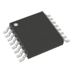 CY2309CZXC-1T

The activity of extra discounts on wholesale prices is in full swing…
Please fill in your contact information and we will send you the latest wholesale price list.






