 ChipApex | Global Electronic Components Supplier

SEARCH
Search Product
Search Post
— IC芯片 | 连接器 | 传感器 | 被动器件 —
Search productSearch post
— IC芯片 | 连接器 | 传感器 | 被动器件 —
Consult the customer manager about the wholesale price.
consultation hotline:86-132-6715-2157
email:[email protected]
Contact the product manager for consultation. One-stop consultation is available.
Do you want a lower wholesale price? Please send us your inquiry and we will reply immediately.
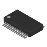
CY23FP12OI is listed in the Clock Buffers, Drivers range at ChipApex. The manufacturer field lists Cypress Semiconductor Corp. Its product description is IC FANOUT BUFFER 28SSOP. Review the specifications below when checking this part for your BOM.
The CY23FP12OI is a fanout buffer and zero delay buffer integrated circuit manufactured by Cypress Semiconductor Corp. It features a 2:12 input-to-output ratio, distributing one clock signal to twelve LVCMOS outputs. The device accepts LVCMOS or LVTTL inputs and operates within supply voltage ranges of 2.375V to 2.625V or 3.135V to 3.465V. Designed for surface mount applications, it is housed in a 28-SSOP package with a width of 5.30mm. The component supports an operating temperature range from -40°C to 85°C.
Verify the specific manufacturing lot date code and RoHS compliance status directly with the supplier, as historical Cypress products may vary in environmental certification. Confirm that the 28-SSOP package dimensions match the target PCB footprint requirements before finalizing procurement orders.
Select this component when a single clock source must drive up to twelve synchronous loads with minimal propagation delay variation. Ensure the system design accommodates the specified dual voltage rails (2.5V/3.3V). Verify that the input signal levels are compatible with LVCMOS or LVTTL standards to guarantee proper logic threshold recognition.
This part belongs to the Cypress clock buffer family, specifically designed for zero-delay buffering applications. It serves as a critical timing element in digital systems where clock integrity and phase alignment are paramount. The 28-SSOP package offers a compact solution for space-constrained designs requiring multiple buffered clock outputs.
Consult official Cypress (now Infineon) documentation for direct pin-compatible replacements within the same series. Verify electrical parameters such as output drive strength and jitter specifications against alternative vendors if cross-sourcing.
Explore related parts through Clock/Timing, Integrated Circuits (ICs), all product categories, ChipApex homepage.
 CY23FP12OI

The activity of extra discounts on wholesale prices is in full swing…
Please fill in your contact information and we will send you the latest wholesale price list.






