 ChipApex | Global Electronic Components Supplier

SEARCH
Search Product
Search Post
— IC芯片 | 连接器 | 传感器 | 被动器件 —
Search productSearch post
— IC芯片 | 连接器 | 传感器 | 被动器件 —
Consult the customer manager about the wholesale price.
consultation hotline:86-132-6715-2157
email:[email protected]
Contact the product manager for consultation. One-stop consultation is available.
Do you want a lower wholesale price? Please send us your inquiry and we will reply immediately.
CY24488ZXC is listed in the Clock Generators, PLLs, Frequency Synthesizers range at ChipApex. The manufacturer field lists Cypress Semiconductor Corp. Its product description is PROCESSOR SPECIFIC CLOCK GENERAT. Review the specifications below when checking this part for your BOM.
The CY24488 is a quad-PLL clock generator featuring a two-wire serial interface. It synthesizes three independent output frequencies plus a buffered reference copy from a single 27 MHz crystal or external clock input. The device supports an optional analog VCXO for frequency pulling via the VIN pin, offering a typical pull range of ±120 ppm. Output drive strength is programmable to minimize EMI, and outputs operate at 3.3 V or 2.5 V. It is housed in a 16-pin TSSOP package.
Verify the specific ordering suffix against Infineon's current catalog to ensure availability and compliance with RoHS standards. Confirm that the required load capacitance matches the programmed register values if using a standard crystal without VCXO functionality. Ensure the serial interface address matches the system design requirements.
Select this component when multiple unrelated clock frequencies are required from a single reference source. Choose the VCXO variant only if precise frequency pulling is necessary; otherwise, disable the feature to relax crystal specifications. Verify that the target application frequencies fall within the supported range of 4.9152 MHz to 148.5 MHz.
The CY24488 belongs to the Cypress Semiconductor clock generator family, now managed by Infineon Technologies. It serves as a direct replacement for non-serial variants like the CY22388 series but adds flexible in-system configuration capabilities. The device is designed for high-performance multimedia applications requiring precise clock synthesis.
The datasheet identifies the CY22388/89/91 as the equivalent parts without a serial port. These can be used if dynamic reconfiguration is not required. Verify pin compatibility and electrical specifications before substitution.
To disable the VCXO, tie the VIN pin to AVDD and program the appropriate register values into the device to select a standard crystal mode.
Upon power-up, all output clocks are off except CLKG, which outputs a copy of the 27 MHz reference clock. The serial programming memory is volatile and must be reconfigured after power cycling.
No, CLKF and CLKG cannot generate independent synthesized frequencies. They can only output a copy of CLKC, CLKD, CLKE, or the 27 MHz reference clock.
Explore related parts through Clock/Timing, Integrated Circuits (ICs), all product categories, ChipApex homepage.
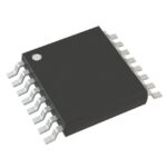 CY24488ZXC

The activity of extra discounts on wholesale prices is in full swing…
Please fill in your contact information and we will send you the latest wholesale price list.





