 ChipApex | Global Electronic Components Supplier
SEARCH
Search Product
Search Post
— IC芯片 | 连接器 | 传感器 | 被动器件 —
Search productSearch post
— IC芯片 | 连接器 | 传感器 | 被动器件 —
Consult the customer manager about the wholesale price.
consultation hotline:86-132-6715-2157
email:[email protected]
Contact the product manager for consultation. One-stop consultation is available.
Do you want a lower wholesale price? Please send us your inquiry and we will reply immediately.
The CY2DP818ZXC is a fanout buffer manufactured by Cypress Semiconductor Corp, designed for clock distribution applications. It features a 1:8 input-to-output ratio and supports differential LVDS, LVPECL, and LVTTL inputs with LVPECL outputs. The device operates at a maximum frequency of 350 MHz within a supply voltage range of 3.135V to 3.465V. Packaged in a 38-TSSOP (38-TFSOP) surface-mount case, it functions reliably across an operating temperature range of 0°C to 70°C.
Verify the specific package variant against the 38-TFSOP specification. Confirm that the required input signal standards (LVDS, LVPECL, or LVTTL) align with the system design. Ensure the operating environment remains within the 0°C to 70°C temperature range and the power supply stays between 3.135V and 3.465V for proper functionality.
Select this component when a single differential or single-ended clock source needs to drive eight LVPECL loads. Verify compatibility with the available input formats (LVDS, LVPECL, LVTTL). Ensure the PCB layout accommodates the 38-TSSOP footprint and that the thermal conditions support the commercial temperature grade.
This part belongs to the Cypress clock buffer family, specifically engineered for high-speed signal integrity. It serves as a critical interface for distributing reference clocks in complex digital architectures where multiple synchronized outputs are required from a single source.
Check for direct pin-compatible alternatives within the same manufacturer's portfolio that match the 1:8 ratio and 350 MHz speed. Verify if other packages like TQFP are available for similar performance requirements.
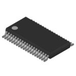 CY2DP818ZXC
The activity of extra discounts on wholesale prices is in full swing…
Please fill in your contact information and we will send you the latest wholesale price list.





