 ChipApex | Global Electronic Components Supplier
SEARCH
Search Product
Search Post
— IC芯片 | 连接器 | 传感器 | 被动器件 —
Search productSearch post
— IC芯片 | 连接器 | 传感器 | 被动器件 —
Consult the customer manager about the wholesale price.
consultation hotline:86-132-6715-2157
email:[email protected]
Contact the product manager for consultation. One-stop consultation is available.
Do you want a lower wholesale price? Please send us your inquiry and we will reply immediately.
The CY2DP818ZXI-2 is a 1:8 clock fanout buffer manufactured by Cypress Semiconductor Corp. It operates on a single 3.3V supply and features a configurable input supporting LVDS, LVPECL, or LVTTL/LVCMOS logic levels via the InConfig pin. The device provides eight pairs of LVPECL differential outputs with individual enable controls. Designed for data communications clock management, it achieves a maximum frequency of 350 MHz with low propagation delay (typical < 4 ns) and low output skew. It is housed in a 38-pin TSSOP package and supports an industrial operating temperature range of -40°C to +85°C.
Verify the ordering suffix 'ZXI' corresponds to the Pb-free Industrial version (-40°C to +85°C) in the 38-Pin TSSOP package. Confirm that the specific revision matches the manufacturer's current documentation, as datasheets may undergo updates. Ensure compatibility with the required input logic configuration via the InConfig pin before integration.
Select this component when a 1:8 fanout ratio is required for LVPECL distribution. The input must be configured for LVDS, LVPECL, or LVTTL using the InConfig pin. Verify that the system can provide the necessary VTT termination voltage for the LVPECL outputs. Ensure the operating environment falls within the specified -40°C to +85°C range for the 'I' suffix variant.
This part belongs to the CY2DP series of network circuits produced using 0.35 micron CMOS technology. The CY2DP818-2 specifically offers a 1:8 fanout capability, distinguishing it from other members of the family that may offer different ratios like 1:4 or 1:6. The 'ZXI' designation indicates the lead-free industrial grade packaging.
Public confirmed substitute part numbers are not available in the provided source material.
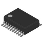 CY2DP818ZXI-2
The activity of extra discounts on wholesale prices is in full swing…
Please fill in your contact information and we will send you the latest wholesale price list.





