 ChipApex | Global Electronic Components Supplier
SEARCH
Search Product
Search Post
— IC芯片 | 连接器 | 传感器 | 被动器件 —
Search productSearch post
— IC芯片 | 连接器 | 传感器 | 被动器件 —
Consult the customer manager about the wholesale price.
consultation hotline:86-132-6715-2157
email:[email protected]
Contact the product manager for consultation. One-stop consultation is available.
Do you want a lower wholesale price? Please send us your inquiry and we will reply immediately.
The CY7B991V-5JIT is a 3.3 V RoboClock low-voltage programmable skew clock buffer manufactured by Infineon Technologies. It features an integrated phase-locked loop (PLL) providing zero input-to-output delay and operates within a frequency range of 3.75 MHz to 80 MHz. The device offers eight LVTTL outputs arranged in four pairs, supporting user-selectable functions including inverted/non-inverted signals, divide-by-two/four operations, and programmable skew up to ±6 time units. It utilizes a 32-pin PLCC package and operates from a single 3.3 V supply with an industrial temperature range of -40°C to +85°C.
Verify the specific suffix 'JIT' against official Infineon documentation to confirm packaging type and temperature grade, as datasheets may list standard variants like JXC or AXI. Confirm availability status, as this component series may be subject to end-of-life notifications or limited production runs.
Select the CY7B991V-5 variant for industrial temperature operation (-40°C to +85°C). Ensure the system clock frequency falls within the 3.75 MHz to 80 MHz range. Verify that the required number of inverted or divided outputs matches the available configuration options for the four output pairs.
The CY7B991V belongs to the RoboClock family of low-voltage programmable skew clock buffers. This series is designed to optimize timing in complex digital systems by allowing flexible clock tree management through internal PLL synchronization and external pin-programmable skew controls.
Check for direct replacements within the CY7B991V series with different suffixes (e.g., JXC, AXI) that match the required package and temperature rating. Cross-reference with other RoboClock devices if pin compatibility or functional equivalence is required.
The maximum operating frequency is 80 MHz, determined by the FS pin configuration.
Skew is controlled via three-level function select inputs (xF0, xF1) for each output pair, allowing delays from -6tU to +6tU relative to the feedback input.
Yes, by connecting a divided output (÷2 or ÷4) to the FB input, the PLL multiplies the REF input frequency at the undivided outputs.
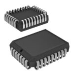 CY7B991V-5JIT
The activity of extra discounts on wholesale prices is in full swing…
Please fill in your contact information and we will send you the latest wholesale price list.





