 ChipApex | Global Electronic Components Supplier
SEARCH
Search Product
Search Post
— IC芯片 | 连接器 | 传感器 | 被动器件 —
Search productSearch post
— IC芯片 | 连接器 | 传感器 | 被动器件 —
Consult the customer manager about the wholesale price.
consultation hotline:86-132-6715-2157
email:[email protected]
Contact the product manager for consultation. One-stop consultation is available.
Do you want a lower wholesale price? Please send us your inquiry and we will reply immediately.
The CYW255OXC is a 200 MHz, 24-output clock buffer designed for PC applications supporting up to four DDR DIMMs or three SDRAM DIMMs. It features one input and 24 outputs, including dedicated pins for feedback and power management. The device operates with dual voltage supplies: VDD3.3_2.5 (3.135V to 3.465V) and VDD2.5 (2.375V to 2.625V). Key electrical parameters include a maximum propagation delay of 10 ns, output skew under 100 ps for DDR mode, and an operating temperature range of 0°C to +70°C. It utilizes a 48-pin SSOP package.
Verify the specific ordering suffix against the manufacturer's current documentation. The 'OXC' suffix indicates a lead-free, commercial-grade variant in a 48-pin SSOP package. Confirm availability status as component lifecycles may change. Ensure the procurement source provides valid traceability for the commercial temperature range specifications.
Select this component when designing systems requiring a single-input, multi-output clock buffer for memory interfaces. Ensure the design accommodates the dual supply requirement: connect VDD3.3_2.5 to 3.3V for SDRAM mode or 2.5V for DDR-only mode. Verify that the PCB layout supports the required bypass capacitance and ferrite bead placement as detailed in the datasheet layout examples.
The CYW255OXC is part of the W255 family of clock buffers originally developed by Silicon Laboratories (formerly Cypress Semiconductor). It serves as a high-speed buffer to distribute reference clocks from chipset synthesizers to multiple memory modules. The device is functionally compatible with other members of the W25x series, differing primarily in packaging and manufacturing revisions.
Publicly confirmed substitute part numbers are not available in the provided documentation. Designers should consult the manufacturer's official cross-reference tools or contact technical support directly for verified replacement options.
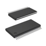 CYW255OXC
The activity of extra discounts on wholesale prices is in full swing…
Please fill in your contact information and we will send you the latest wholesale price list.






