ChipApex | Global Electronic Components Supplier
SEARCH
Search Product
Search Post
— IC芯片 | 连接器 | 传感器 | 被动器件 —
Search productSearch post
— IC芯片 | 连接器 | 传感器 | 被动器件 —
Consult the customer manager about the wholesale price.
consultation hotline:86-132-6715-2157
email:[email protected]
Contact the product manager for consultation. One-stop consultation is available.
Do you want a lower wholesale price? Please send us your inquiry and we will reply immediately.
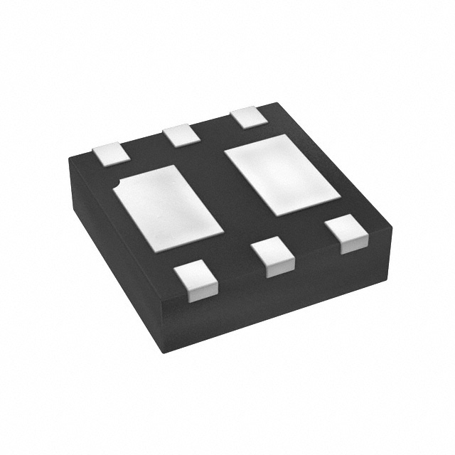
The DMC2053UFDBQ-7 is a complementary pair enhancement mode MOSFET manufactured by Diodes Incorporated. It integrates an N-channel and P-channel device within a U-DFN2020-6 package. The N-channel component features a drain-source voltage of 20V, with maximum on-resistance values of 35mΩ at VGS=4.5V and 43mΩ at VGS=2.5V. Continuous drain current reaches 4.6A at 25°C. The P-channel counterpart provides -20V breakdown, with on-resistance of 75mΩ at VGS=-4.5V and 110mΩ at VGS=-2.5V, supporting continuous currents up to -3.1A. Total power dissipation is rated at 0.82W.
Verify the specific ordering suffix when sourcing components. The datasheet identifies DMC2053UFDBQ-7 as the variant supplied in 3,000-unit tape and reel packaging. Confirm that the received parts match the required packing quantity and carrier type specified for your assembly line equipment. Cross-reference the manufacturer part number against official distributor catalogs to ensure authenticity and traceability.
Select this component for designs requiring a small form factor complementary MOSFET pair. Ensure the gate drive voltage aligns with the specified thresholds for optimal RDS(ON) performance. Evaluate thermal constraints carefully, as the U-DFN2020-6 package has limited heat dissipation capabilities compared to larger packages. Verify that the application current does not exceed the continuous ratings defined in the electrical characteristics table.
This device belongs to Diodes Incorporated's complementary MOSFET portfolio, specifically engineered for space-constrained power circuits. The U-DFN2020-6 package allows for dense PCB layouts while maintaining robust electrical isolation between the N-channel and P-channel elements. It serves as a direct replacement for discrete dual-MOSFET solutions in modern portable electronics.
Check pinout compatibility before substitution. Verify that any alternative component matches the 20V rating and similar on-resistance specifications. Ensure the replacement package fits the existing footprint without mechanical interference.
The operating and storage temperature range extends from -55°C to +150°C.
Yes, it is totally lead-free, fully RoHS compliant, and halogen- and antimony-free.
The typical input capacitance (Ciss) is 369pF at VDS=10V and f=1.0MHz.
 DMC2053UFDBQ-7
The activity of extra discounts on wholesale prices is in full swing…
Please fill in your contact information and we will send you the latest wholesale price list.