 ChipApex | Global Electronic Components Supplier
SEARCH
Search Product
Search Post
— IC芯片 | 连接器 | 传感器 | 被动器件 —
Search productSearch post
— IC芯片 | 连接器 | 传感器 | 被动器件 —
Consult the customer manager about the wholesale price.
consultation hotline:86-132-6715-2157
email:[email protected]
Contact the product manager for consultation. One-stop consultation is available.
Do you want a lower wholesale price? Please send us your inquiry and we will reply immediately.
The DMC3732UVTQ is a complementary pair enhancement mode MOSFET manufactured by Diodes Incorporated. It integrates an N-channel device (Q1) and a P-channel device (Q2) in a single TSOT26 package. The Q1 offers a drain-source voltage of 30V, with on-resistance values of 460mΩ at VGS=4.5V and 560mΩ at VGS=2.5V. The Q2 provides -30V breakdown, with on-resistance of 1000mΩ at VGS=-4.5V and 1500mΩ at VGS=-2.5V. Continuous drain currents are 1.1A for Q1 and -0.7A for Q2 at +25°C. Power dissipation reaches 0.83W on a 1-inch square copper plate.
Verify the specific ordering suffix when purchasing. The suffix '-7' indicates a tape and reel quantity of 3,000 units, while '-13' denotes 10,000 units per reel. Confirm that the component meets RoHS 2 and RoHS 3 directives if environmental compliance is required for your assembly process.
Select this component for space-constrained designs requiring a matched N-P channel pair. Ensure the gate drive voltage aligns with the specified thresholds; the device exhibits lower on-resistance at higher gate voltages like 4.5V compared to 2.5V or 1.8V. Consider the thermal resistance of 230°C/W on standard FR-4 substrates when calculating heat dissipation limits.
This part belongs to the DMC series of complementary MOSFETs from Diodes Incorporated. It serves as a compact solution for replacing discrete N-channel and P-channel transistors in dual-transistor configurations. The TSOT26 package allows for automated surface-mount assembly, supporting high-volume manufacturing requirements.
Publicly confirmed substitute part numbers are not available in the provided documentation. Verify pinout compatibility and electrical parameters against existing designs before substituting with other complementary MOSFET pairs.
The maximum continuous drain current for the N-channel device (Q1) is 1.1A at a case temperature of +25°C.
Yes, the DMC3732UVTQ is AEC-Q101 qualified, PPAP capable, and manufactured in IATF 16949 certified facilities, making it suitable for automotive applications requiring specific change control.
The on-resistance decreases as the gate voltage increases. For the N-channel device, RDS(ON) is 460mΩ at VGS=4.5V, but rises to 560mΩ at VGS=2.5V and 730mΩ at VGS=1.8V.
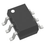 DMC3732UVTQ-7
The activity of extra discounts on wholesale prices is in full swing…
Please fill in your contact information and we will send you the latest wholesale price list.





