 ChipApex | Global Electronic Components Supplier
SEARCH
Search Product
Search Post
— IC芯片 | 连接器 | 传感器 | 被动器件 —
Search productSearch post
— IC芯片 | 连接器 | 传感器 | 被动器件 —
Consult the customer manager about the wholesale price.
consultation hotline:86-132-6715-2157
email:[email protected]
Contact the product manager for consultation. One-stop consultation is available.
Do you want a lower wholesale price? Please send us your inquiry and we will reply immediately.
The DMGD7N45SSD-13 is a dual N-channel enhancement mode MOSFET manufactured by Diodes Incorporated. It features a drain-source breakdown voltage (V(BR)DSS) of 450 V and a maximum static drain-source on-resistance (RDS(ON)) of 4 Ω at VGS = 10 V. The device supports a continuous drain current (ID) of 0.85 A at +25°C and a pulsed drain current (IDM) of 2.2 A. Total power dissipation (PD) is rated at 1.64 W, with a thermal resistance junction-to-ambient (RθJA) of 78 °C/W. Operating temperature ranges from -55 °C to +150 °C.
Verify the component against official datasheet DS36011 Rev. 7-2 specifications before integration. Confirm that the SO-8 package dimensions and pinout match your PCB layout requirements. Ensure environmental compliance aligns with project needs, as the device is lead-free, RoHS compliant, and halogen/antimony free. Validate thermal management strategies given the 1.64 W power dissipation limit in steady-state conditions.
Select this component when high voltage isolation up to 450 V is required in a compact dual configuration. The 4 Ω RDS(ON) makes it appropriate for lower current switching tasks rather than high-power conduction. Consider the 78 °C/W thermal resistance for heat dissipation planning. Verify gate threshold voltage compatibility with your control logic levels, which typically range between 3.5 V and 4.5 V.
This part belongs to Diodes Incorporated's dual MOSFET portfolio, designed to save board space compared to discrete single-channel devices. The 'SSD' suffix indicates the SO-8 surface-mount package and specific tape-and-reel packaging format. It serves as a complementary solution for circuits requiring two isolated N-channel switches within a single footprint.
Direct replacements must match the 450 V rating, SO-8 package, and dual N-channel configuration. Verify that any substitute maintains similar RDS(ON) and Qg values to ensure equivalent switching performance and thermal behavior in existing designs.
The maximum pulsed drain current (IDM) is 2.2 A, measured with a 10 µs pulse duration and a 1% duty cycle.
Yes, the device is qualified to AEC-Q101 standards, indicating its suitability for high-reliability automotive environments.
The total gate charge (Qg) is typically 6.9 nC, measured at VDS = 360 V, ID = 0.7 A, and VGS = 10 V.
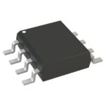 DMGD7N45SSD-13
The activity of extra discounts on wholesale prices is in full swing…
Please fill in your contact information and we will send you the latest wholesale price list.





