ChipApex | Global Electronic Components Supplier
SEARCH
Search Product
Search Post
— IC芯片 | 连接器 | 传感器 | 被动器件 —
Search productSearch post
— IC芯片 | 连接器 | 传感器 | 被动器件 —
Consult the customer manager about the wholesale price.
consultation hotline:86-132-6715-2157
email:[email protected]
Contact the product manager for consultation. One-stop consultation is available.
Do you want a lower wholesale price? Please send us your inquiry and we will reply immediately.
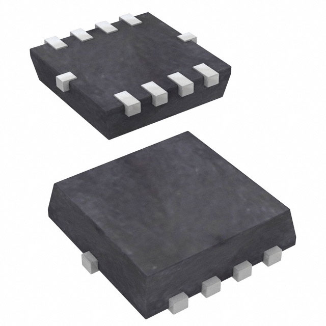
The DMN10H220LDV is a dual N-channel enhancement mode MOSFET manufactured by Diodes Incorporated. It features a maximum drain-source voltage (BVDSS) of 100 V and a gate-source voltage (VGSS) rating of ±20 V. The device provides a continuous drain current (ID) of 10.5 A at a case temperature of +25°C, with a pulsed drain current (IDM) capability of 42 A. Static drain-source on-resistance (RDS(ON)) is specified as a maximum of 222 mΩ at VGS = 10 V and ID = 2 A, and 270 mΩ at VGS = 4.5 V and ID = 1 A. Total gate charge (Qg) reaches 6.7 nC at VGS = 10 V. The component operates within a junction temperature range of -55°C to +150°C and utilizes the PowerDI3333-8 surface-mount package.
Verify the specific ordering suffix when sourcing components. The datasheet lists both DMN10H220LDV-7 and DMN10H220LDV-13 variants. Confirm that the received part matches the required packaging quantity and reel specifications for your assembly line. Ensure compliance with moisture sensitivity level 1 requirements during storage and handling.
Select this component for designs requiring a dual N-channel topology within a small footprint. Evaluate thermal constraints carefully, as total power dissipation is limited to 1.8 W at ambient temperature. Verify that the gate drive voltage meets the minimum threshold for optimal RDS(ON) performance. Consider the 100 V breakdown voltage limit when designing for transient voltage spikes.
This device belongs to the DMN10 series of dual MOSFETs from Diodes Incorporated. It shares the PowerDI3333-8 package form factor with other members of the family but differs in electrical ratings such as on-resistance and current capacity. The dual configuration allows for space-saving implementations compared to using discrete single-channel devices.
Direct substitutes include other DMN10 series parts like DMN10H099SFG-7 or DMN10H170SFDE-13, provided they fit the PowerDI3333-8 footprint. Verify pinout compatibility and ensure the replacement's RDS(ON) and current ratings meet or exceed the original design requirements.
The maximum avalanche energy (EAS) is rated at 1.1 mJ based on a low-frequency inductance of 0.1 mH.
Yes, the datasheet confirms that 100% of production units undergo Unclamped Inductive Switching (UIS) testing.
The typical body diode reverse recovery charge (QRR) is 11 nC, measured at a source current of 1.1 A and a rate of change of current of 100 A/μs.
 DMN10H220LDV-13
The activity of extra discounts on wholesale prices is in full swing…
Please fill in your contact information and we will send you the latest wholesale price list.