ChipApex | Global Electronic Components Supplier

SEARCH
Search Product
Search Post
— IC芯片 | 连接器 | 传感器 | 被动器件 —
Search productSearch post
— IC芯片 | 连接器 | 传感器 | 被动器件 —
Consult the customer manager about the wholesale price.
consultation hotline:86-132-6715-2157
email:[email protected]
Contact the product manager for consultation. One-stop consultation is available.
Do you want a lower wholesale price? Please send us your inquiry and we will reply immediately.
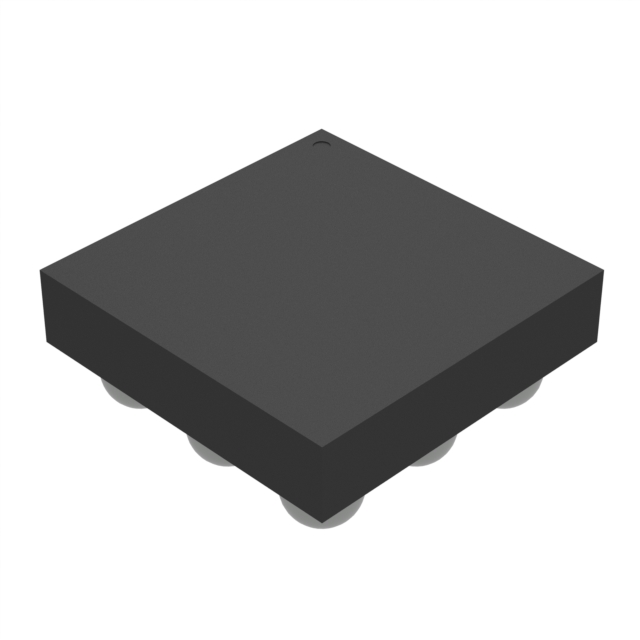
The DMP1007UCB9-7 is a P-channel enhancement mode MOSFET utilizing third-generation lateral MOSFET (LD-MOS) technology. It features an ultra-low on-state resistance of 5.7mΩ at VGS = -4.5V and a gate charge of 8.2nC for fast switching. The device supports a drain-source voltage of -8V, continuous drain current up to -13.2A, and operates within a junction temperature range of -55°C to +150°C. Packaged in a compact U-WLB1515-9 footprint measuring 1.5mm x 1.5mm with a height of 0.62mm.
Verify the specific ordering suffix '-7' corresponds to the 3,000-unit tape and reel packaging configuration. Confirm that the component meets RoHS 2/3 compliance standards and ensure the application environment remains within the specified -55°C to +150°C operating temperature limits. Cross-reference the datasheet revision for any updates to mechanical dimensions or electrical characteristics prior to finalizing procurement orders.
Select this component when high efficiency and rapid switching are required in space-constrained designs. The low RDS(ON) value reduces conduction losses, making it suitable for battery-powered applications. Ensure the gate drive voltage aligns with the -4.5V specification to achieve optimal performance. Consider the thermal management requirements based on the specific PCB copper area utilized during mounting.
This part belongs to Diodes Incorporated's DMP series of P-channel MOSFETs. It utilizes the U-WLB1515-9 package, also known as Chip-Scale Package (CSP), which provides a highly compact form factor. The device is designed specifically for high-efficiency power transfer applications where minimizing both electrical and physical footprint is critical.
Consult official Diodes Incorporated documentation for verified substitute part numbers. Do not assume cross-compatibility with other manufacturers' devices without validating pin configurations, electrical ratings, and thermal characteristics against the original specifications.
The typical gate threshold voltage (VGS(TH)) is -0.6V, with a maximum of -1.1V under standard test conditions.
Yes, the datasheet specifies that the component includes ESD protection for the gate terminal.
 DMP1007UCB9-7

The activity of extra discounts on wholesale prices is in full swing…
Please fill in your contact information and we will send you the latest wholesale price list.