ChipApex | Global Electronic Components Supplier

SEARCH
Search Product
Search Post
— IC芯片 | 连接器 | 传感器 | 被动器件 —
Search productSearch post
— IC芯片 | 连接器 | 传感器 | 被动器件 —
Consult the customer manager about the wholesale price.
consultation hotline:86-132-6715-2157
email:[email protected]
Contact the product manager for consultation. One-stop consultation is available.
Do you want a lower wholesale price? Please send us your inquiry and we will reply immediately.
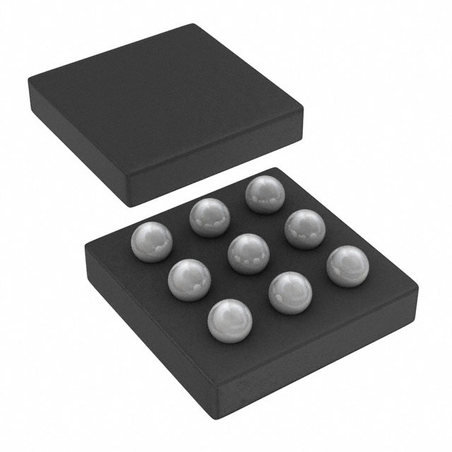
The DMP1008UCB9-7 is a P-channel enhancement mode MOSFET utilizing third-generation LD-MOS technology. It features an -8V drain-source voltage and a maximum on-resistance of 5.7mΩ at VGS = -4.5V. The device supports a continuous drain current of -13.2A at +25°C and operates within a junction temperature range of -55°C to +150°C. Packaged in a U-WLB1515-9 chip-scale format, it offers low thermal impedance and ultra-fast switching characteristics.
Verify component authenticity through authorized Diodes Incorporated channels or certified distributors. Confirm package marking codes match the U-WLB1515-9 specification and date code formats. Ensure compliance with RoHS 3 and halogen-free requirements as defined by the manufacturer. Validate that storage conditions adhere to J-STD-020 moisture sensitivity level 1 guidelines prior to soldering.
Select this component for applications requiring high efficiency in compact form factors. The low RDS(ON) minimizes conduction losses, while the CSP footprint maximizes board space utilization. Consider the -8V rating for low-voltage power rails. Evaluate thermal management needs based on the specific PCB copper area and ambient operating temperatures.
This part belongs to the DMP series of lateral MOSFETs from Diodes Incorporated. It represents a generation of devices optimized for high-density power management solutions. The U-WLB1515-9 package is designed to replace larger traditional packages while maintaining robust electrical performance and thermal dissipation capabilities.
Direct substitutes must match the -8V rating, P-channel configuration, and U-WLB1515-9 footprint. Verify equivalent RDS(ON) and Qg values to ensure identical switching performance. Consult official cross-reference lists for confirmed compatible replacements.
 DMP1008UCB9-7

The activity of extra discounts on wholesale prices is in full swing…
Please fill in your contact information and we will send you the latest wholesale price list.