 ChipApex | Global Electronic Components Supplier

SEARCH
Search Product
Search Post
— IC芯片 | 连接器 | 传感器 | 被动器件 —
Search productSearch post
— IC芯片 | 连接器 | 传感器 | 被动器件 —
Consult the customer manager about the wholesale price.
consultation hotline:86-132-6715-2157
email:[email protected]
Contact the product manager for consultation. One-stop consultation is available.
Do you want a lower wholesale price? Please send us your inquiry and we will reply immediately.
The DMP2040USD-13 is a dual P-channel enhancement mode MOSFET manufactured by Diodes Incorporated in an SO-8 surface-mount package. It features a drain-source voltage rating of -20V and a continuous drain current of -6.5A at +25°C. The device offers a maximum on-resistance of 33mΩ at VGS = -4.5V and 52mΩ at VGS = -2.5V. Key electrical parameters include a gate-source voltage limit of ±12V, a total power dissipation of 1.1W, and a junction-to-ambient thermal resistance of 108°C/W. Operating temperatures range from -55°C to +150°C.
Verify the specific ordering suffix '-13' corresponds to the 2500-unit tape and reel packaging format. Confirm that the component meets all applicable environmental directives, including RoHS compliance and halogen-free requirements, as specified in the manufacturer's documentation. Ensure compatibility with standard SO-8 footprint layouts during procurement planning.
Select this component for applications requiring dual P-channel control within a compact SO-8 footprint. Evaluate the thermal performance against the 108°C/W junction-to-ambient resistance, particularly for steady-state operations on FR-4 substrates. Consider the -20V breakdown voltage and -6.5A continuous current limits when designing power stages to ensure reliable operation under expected load conditions.
This part belongs to the DMP2040 series of advanced generation MOSFETs designed to balance low on-resistance with superior switching performance. Manufactured by Diodes Incorporated, it utilizes a molded plastic case with matte tin annealed terminals. The product marking includes the code 'P2040UD' along with date codes for traceability.
Direct substitutes include other dual P-channel MOSFETs in SO-8 packages with comparable -20V ratings and similar RDS(ON) specifications. Verify pinout compatibility and thermal characteristics before substitution.
The absolute maximum gate-source voltage (VGSS) is rated at ±12V.
The on-resistance increases as the junction temperature rises, as illustrated in the typical on-resistance vs. junction temperature graphs provided in the datasheet.
Yes, the typical body diode reverse recovery time (tRR) is 9.8ns when tested at IF = -8.9A and di/dt = -100A/μs.
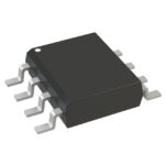 DMP2040USD-13

The activity of extra discounts on wholesale prices is in full swing…
Please fill in your contact information and we will send you the latest wholesale price list.





