 ChipApex | Global Electronic Components Supplier

SEARCH
Search Product
Search Post
— IC芯片 | 连接器 | 传感器 | 被动器件 —
Search productSearch post
— IC芯片 | 连接器 | 传感器 | 被动器件 —
Consult the customer manager about the wholesale price.
consultation hotline:86-132-6715-2157
email:[email protected]
Contact the product manager for consultation. One-stop consultation is available.
Do you want a lower wholesale price? Please send us your inquiry and we will reply immediately.
The DMP2110UFDBQ-13 is a dual P-channel enhancement mode MOSFET manufactured by Diodes Incorporated. It features a maximum drain-source voltage (BVDSS) of -20V and a typical static drain-source on-resistance (RDS(ON)) of 75mΩ at VGS = -4.5V, rising to 110mΩ at VGS = -2.5V. The device supports a continuous drain current (ID) of -3.2A at +25°C. Packaged in a U-DFN2020-6 (Type B) footprint measuring 4mm² with a maximum height of 0.6mm, it offers low input capacitance (Ciss: 443pF) and total gate charge (Qg: 6.0nC @ VGS=-4.5V).
Verify the ordering suffix '-13' corresponds to the 10,000-unit tape and reel carrier quantity as specified in the manufacturer's ordering information. Confirm that the U-DFN2020-6 (Type B) package dimensions align with the PCB pad layout requirements. Ensure compliance with IATF 16949 manufacturing standards if the application demands automotive-grade traceability and quality control protocols.
Select this component when a dual P-channel solution is required in a minimal surface area footprint. The device is appropriate for designs needing low on-resistance at standard logic-level gate voltages (-4.5V or -2.5V). Consider the thermal resistance characteristics and the 0.6mm profile constraint during mechanical integration. Verify that the -20V breakdown voltage meets the system's maximum operating voltage requirements.
This part belongs to the DMP2110 series of dual P-channel enhancement mode MOSFETs from Diodes Incorporated. It shares the core electrical specifications of the single-channel DMP2110U variants but integrates two independent channels into a single U-DFN2020-6 package. This consolidation reduces board space compared to using discrete single-channel devices.
DMP2110UFDBQ-7
Yes, the DMP2110UFDBQ is AEC-Q101 qualified, PPAP capable, and manufactured in IATF 16949 certified facilities, making it suitable for automotive applications requiring specific change control.
The maximum height of the U-DFN2020-6 (Type B) package is 0.6mm.
The typical RDS(ON) is 75mΩ at VGS = -4.5V and increases to 110mΩ at VGS = -2.5V under specified test conditions.
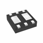 DMP2110UFDBQ-13

The activity of extra discounts on wholesale prices is in full swing…
Please fill in your contact information and we will send you the latest wholesale price list.





