 ChipApex | Global Electronic Components Supplier
SEARCH
Search Product
Search Post
— IC芯片 | 连接器 | 传感器 | 被动器件 —
Search productSearch post
— IC芯片 | 连接器 | 传感器 | 被动器件 —
Consult the customer manager about the wholesale price.
consultation hotline:86-132-6715-2157
email:[email protected]
Contact the product manager for consultation. One-stop consultation is available.
Do you want a lower wholesale price? Please send us your inquiry and we will reply immediately.
The DMP2900UW-13 is a P-channel enhancement mode MOSFET manufactured by Diodes Incorporated. It features a maximum drain-source voltage (BVDSS) of -20V and operates within a junction temperature range of -55°C to +150°C. The device provides a continuous drain current (ID) of -0.6A at TA = +25°C with a steady-state total power dissipation (PD) of 0.3W. Static drain-source on-resistance (RDS(ON)) values are specified as 750mΩ at VGS = -4.5V, 1050mΩ at VGS = -2.5V, and 1500mΩ at VGS = -1.8V. The gate threshold voltage (VGS(TH)) ranges from -0.5V to -1.0V. The component utilizes an SOT323 surface-mount package.
Verify the specific ordering suffix '-13' corresponds to the 10,000-unit tape and reel packaging configuration. Confirm that the requested part number matches the exact electrical ratings and thermal characteristics required for the target application environment. Ensure compliance with applicable automotive or industrial standards if necessary, as standard versions may differ from qualified variants.
Select this component for circuits requiring a compact P-channel switch with a -20V rating. Evaluate the RDS(ON) requirements against available gate drive voltages (-1.8V, -2.5V, or -4.5V) to ensure adequate current handling. Consider the thermal resistance of 393 °C/W for heat dissipation calculations in steady-state conditions.
This component belongs to the DMP2900 series of P-channel enhancement mode MOSFETs produced by Diodes Incorporated under the DiodesZetex brand. It is designed for surface-mount assembly using the SOT323 case style. The product line emphasizes low on-resistance and fast switching capabilities suitable for portable and battery-powered electronics.
DMP2900UW-7 is an equivalent part number offering identical electrical specifications but packaged in a 3,000-unit tape and reel quantity instead of 10,000 units.
The maximum body diode forward current (IS) is rated at -0.45 A.
The typical turn-off delay time (tD(OFF)) is 213 ns under test conditions of VDD = -10V, VGS = -4.5V, RL = 47Ω, RG = 10Ω, and ID = -200mA.
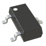 DMP2900UW-13
The activity of extra discounts on wholesale prices is in full swing…
Please fill in your contact information and we will send you the latest wholesale price list.





