 ChipApex | Global Electronic Components Supplier
SEARCH
Search Product
Search Post
— IC芯片 | 连接器 | 传感器 | 被动器件 —
Search productSearch post
— IC芯片 | 连接器 | 传感器 | 被动器件 —
Consult the customer manager about the wholesale price.
consultation hotline:86-132-6715-2157
email:[email protected]
Contact the product manager for consultation. One-stop consultation is available.
Do you want a lower wholesale price? Please send us your inquiry and we will reply immediately.
The DMP3097L-13 is a P-channel enhancement mode MOSFET manufactured by Diodes Incorporated in an SOT-23 surface-mount package. It features a drain-source voltage (V_DSS) of -30 V and a maximum continuous drain current (I_D) of -3.9 A at +25°C. The device exhibits a low on-state resistance (R_DS(ON)) of 65 mΩ at V_GS = -10 V and 99 mΩ at V_GS = -4.5 V. Key electrical parameters include a gate threshold voltage (V_GS(TH)) ranging from -1.0 V to -2.1 V, total gate charge (Q_g) of 6.6 nC at V_GS = -4.5 V, and input capacitance (C_iss) of 563 pF. The component supports a junction temperature range of -55°C to +150°C.
Verify the specific ordering suffix '-13' corresponds to the 10,000-unit tape and reel packaging configuration as defined in the manufacturer's documentation. Confirm that the component meets RoHS 2 and RoHS 3 compliance standards, including halogen-free and antimony-free specifications if required by the project constraints. Ensure the procurement channel is authorized to guarantee product authenticity and traceability.
Select this component when a compact SOT-23 footprint is required for P-channel switching with a -30 V rating. The low R_DS(ON) values at both -10 V and -4.5 V gate drives make it suitable for logic-level control interfaces. Evaluate the thermal resistance and power dissipation limits against the expected load current and ambient operating conditions to ensure reliable operation within the specified temperature range.
This part belongs to the DMP3097L series of P-channel enhancement mode MOSFETs produced by Diodes Incorporated. The family focuses on optimizing the balance between conduction losses and switching dynamics. The standard SOT-23 case provides a cost-effective and space-efficient solution for general-purpose discrete semiconductor applications requiring moderate current handling capabilities.
Direct substitutes must match the -30 V drain-source voltage, P-channel topology, and SOT-23-3 package outline. Verify that alternative components offer comparable R_DS(ON) values at -10 V and -4.5 V gate voltages to maintain circuit efficiency. Ensure pinout compatibility (Drain, Gate, Source) to prevent board redesign during replacement.
The maximum pulsed drain current (I_DM) is rated at -20 A, based on a 10 µs pulse duration with a 1% duty cycle.
The gate threshold voltage (V_GS(TH)) typically shifts negatively as the junction temperature increases, as illustrated in the typical transfer characteristic graphs provided in the datasheet.
Standard production units are not explicitly qualified for automotive use. For applications requiring AEC-Q100/101/200 qualification and IATF 16949 manufacturing, customers must contact Diodes Incorporated directly.
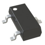 DMP3097L-13
The activity of extra discounts on wholesale prices is in full swing…
Please fill in your contact information and we will send you the latest wholesale price list.





