 ChipApex | Global Electronic Components Supplier
SEARCH
Search Product
Search Post
— IC芯片 | 连接器 | 传感器 | 被动器件 —
Search productSearch post
— IC芯片 | 连接器 | 传感器 | 被动器件 —
Consult the customer manager about the wholesale price.
consultation hotline:86-132-6715-2157
email:[email protected]
Contact the product manager for consultation. One-stop consultation is available.
Do you want a lower wholesale price? Please send us your inquiry and we will reply immediately.
The DMP3099L-13 is a P-channel enhancement mode MOSFET manufactured by Diodes Incorporated. It features a drain-source voltage (V_DSS) of -30 V and a continuous drain current (I_D) of -3.8 A at +25°C ambient temperature. The device offers a maximum on-resistance (R_DS(ON)) of 65 mΩ at V_GS = -10 V and -3.8 A, or 99 mΩ at V_GS = -4.5 V and -3.0 A. Total power dissipation is rated at 1.08 W with a thermal resistance (R_θJA) of 115 °C/W. Operating junction temperature ranges from -55°C to +150°C. The component is housed in a standard SOT-23 package.
Verify the specific ordering suffix '-13' corresponds to the 10,000-unit tape and reel packaging configuration as defined in the manufacturer's documentation. Confirm that the required automotive compliance is not needed; if automotive qualification is necessary, the separate datasheet for part number DMP3099LQ must be referenced instead of this standard commercial grade variant.
Select this component when a compact SOT-23 footprint is required for P-channel switching applications operating within a 30 V limit. Ensure the driving circuit can provide sufficient gate-source voltage to achieve the desired R_DS(ON), noting the higher resistance at lower drive voltages. Evaluate thermal management requirements against the 115 °C/W junction-to-ambient rating for the intended PCB copper pad area.
This device belongs to the DMP3099 series of P-channel enhancement mode MOSFETs produced by Diodes Incorporated. The series is engineered for power management efficiency. The DMP3099L-13 specifically denotes the standard commercial version packaged in a tape and reel format, distinct from the automotive-compliant DMP3099LQ variant which follows a separate datasheet specification.
For automotive-grade requirements, consider the DMP3099LQ. Other series members like DMP3098LSS-13 offer different packages and current ratings but share similar voltage specifications.
The maximum pulsed drain current (I_DM) is rated at -11 A, provided the pulse width is less than or equal to 10 µs and the duty cycle does not exceed 1%.
The static drain-source on-resistance (R_DS(ON)) is specified as a maximum of 65 mΩ at V_GS = -10 V and I_D = -3.8 A. At a lower drive voltage of V_GS = -4.5 V and I_D = -3.0 A, the maximum R_DS(ON) increases to 99 mΩ.
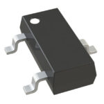 DMP3099L-13
The activity of extra discounts on wholesale prices is in full swing…
Please fill in your contact information and we will send you the latest wholesale price list.





