 ChipApex | Global Electronic Components Supplier
SEARCH
Search Product
Search Post
— IC芯片 | 连接器 | 传感器 | 被动器件 —
Search productSearch post
— IC芯片 | 连接器 | 传感器 | 被动器件 —
Consult the customer manager about the wholesale price.
consultation hotline:86-132-6715-2157
email:[email protected]
Contact the product manager for consultation. One-stop consultation is available.
Do you want a lower wholesale price? Please send us your inquiry and we will reply immediately.
The DN2535N5-G is an N-Channel Depletion-mode Vertical DMOS FET manufactured by Microchip Technology. It features a 350 V drain-to-source breakdown voltage and a maximum on-resistance of 25 Ω at 120 mA. The device supports a continuous drain current of 500 mA and dissipates up to 15 W in the TO-220 package. Operating temperatures range from -55°C to +150°C, with a gate-to-source voltage limit of ±20 V.
Verify the specific suffix 'N5' corresponds to the 3-lead TO-220 package configuration required for your design. Confirm that the 'G' designation indicates lead-free and RoHS-compliant packaging as specified in the product identification system. Ensure the procurement channel sources directly from authorized distributors to guarantee component authenticity and traceability.
Select this component when a normally-on (depletion-mode) switch or amplifier is required with high input impedance. The TO-220 package provides sufficient thermal dissipation for applications requiring up to 15 W power handling. Verify that the 350 V breakdown voltage meets the circuit's peak voltage requirements and that the 25 Ω on-resistance aligns with acceptable conduction losses.
This part belongs to the DN2535 family of N-Channel Depletion-mode Vertical DMOS FETs. The DN2535N5-G specifically denotes the version packaged in a 3-lead TO-220 housing with lead-free compliance. Other variants in the series include the TO-92 package options, offering flexibility for different thermal and spatial constraints while maintaining identical electrical performance characteristics.
Direct substitutes within the same family include DN2535N3-G (TO-92 package). Cross-brand replacements require matching depletion-mode operation, 350 V BVDSX, and comparable RDS(ON) specifications. Verify pinout compatibility, particularly for the TO-220 variant where Pin 4 is Drain.
The DN2535N5-G is a depletion-mode (normally-on) transistor, meaning it conducts current between the drain and source when the gate-to-source voltage is zero.
The device is free from thermal runaway and thermally induced secondary breakdown, a characteristic inherent to its MOS structure.
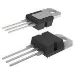 DN2535N5-G
The activity of extra discounts on wholesale prices is in full swing…
Please fill in your contact information and we will send you the latest wholesale price list.





