 ChipApex | Global Electronic Components Supplier

SEARCH
Search Product
Search Post
— IC芯片 | 连接器 | 传感器 | 被动器件 —
Search productSearch post
— IC芯片 | 连接器 | 传感器 | 被动器件 —
Consult the customer manager about the wholesale price.
consultation hotline:86-132-6715-2157
email:[email protected]
Contact the product manager for consultation. One-stop consultation is available.
Do you want a lower wholesale price? Please send us your inquiry and we will reply immediately.
DS8023-RRX+T&R is listed in the Specialized range at ChipApex. The manufacturer field lists Analog Devices Inc./Maxim Integrated. Its product description is IC INTERFACE SPECIALIZED 28SOIC. Review the specifications below when checking this part for your BOM.
The DS8023-RRX+T&R is a smart card interface IC designed for ISO 7816, EMV, and GSM applications. It supports 5V, 3V, and 1.8V cards with an internal charge pump generating VCC up to 80mA at 5V, 65mA at 3V, or 30mA at 1.8V. Operating from a digital supply (VDD) of 2.7V to 6.0V and a charge-pump supply (VDDA) of 3.0V to 6.0V, it features ultra-low stop-mode current below 10nA. The device includes ±8kV ESD protection, automatic activation/deactivation sequencing, and flexible clock generation via external crystal inputs up to 20MHz.
Verify the specific suffix RRX corresponds to the SO package variant when sourcing. Confirm RoHS compliance status through official manufacturer documentation as ordering suffixes may indicate lead-free specifications. Ensure the component meets the required temperature range of -40°C to +85°C for your application environment.
Select this component for designs requiring a single-chip solution for multiple smart card voltage standards. Ensure the host microcontroller operates within the compatible VDD range. Verify that the PCB layout allows for proper decoupling of VDD and VDDA supplies to maintain signal integrity and minimize jitter on the clock line.
This part belongs to the Maxim Integrated DS8023 family of smart card interfaces. It serves as a direct replacement for older models like the TDA8024 with minimal hardware changes. The RRX suffix specifically denotes the 28-pin Small Outline (SO) package option within the broader product line.
The DS8023 is documented as a compatible replacement for the NXP TDA8024. When substituting, verify that the pinout compatibility holds for the specific package type and update firmware to support the ultra-low-power stop mode if utilized.
The device uses PRES and PRES pins to detect card insertion. An internal debounce circuit waits approximately 8ms before asserting the OFF output high to confirm presence.
Stop mode is entered by setting CMDVCC, 5V/3V, and 1_8V pins to logic-high simultaneously while the interface is inactive. This disables all internal analog circuits to achieve current consumption below 10nA.
Yes, it can operate from a single input voltage. The internal charge pump generates the necessary higher voltages for the card supply (VCC) from the VDD and VDDA inputs.
Explore related parts through Interface, Integrated Circuits (ICs), all product categories, ChipApex homepage.
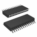 DS8023-RRX+T&R

The activity of extra discounts on wholesale prices is in full swing…
Please fill in your contact information and we will send you the latest wholesale price list.






