 ChipApex | Global Electronic Components Supplier
SEARCH
Search Product
Search Post
— IC芯片 | 连接器 | 传感器 | 被动器件 —
Search productSearch post
— IC芯片 | 连接器 | 传感器 | 被动器件 —
Consult the customer manager about the wholesale price.
consultation hotline:86-132-6715-2157
email:[email protected]
Contact the product manager for consultation. One-stop consultation is available.
Do you want a lower wholesale price? Please send us your inquiry and we will reply immediately.
The DS92LV1212TMSAX is a Texas Instruments LVDS interface integrated circuit designed as a 10-bit bus deserializer. It operates within a frequency range of 16 MHz to 40 MHz and features embedded clock recovery for random lock applications. The device accepts Low Voltage Differential Signaling (LVDS) inputs and converts them into parallel outputs compatible with LVCMOS or LVTTL logic levels. It is housed in a 28-pin SSOP package suitable for surface mount technology. The component supports a supply voltage range from 3 V to 3.6 V, with a typical operating voltage of 3.3 V, and functions reliably across an industrial temperature range of -40°C to +85°C.
Verify the specific suffix 'TMSAX' against the manufacturer's current datasheet to confirm pinout and electrical characteristics match your design requirements. Ensure that the 28-SSOP package dimensions align with your PCB footprint constraints. Confirm RoHS compliance status through official documentation before finalizing procurement decisions.
Select this component when a 10-bit parallel output is required from an LVDS source within the 16-40 MHz bandwidth. Consider the embedded clock recovery feature if minimizing trace count between transmitter and receiver is critical. Verify that the input voltage swing and common-mode range are compatible with the driving LVDS source specifications.
This part belongs to the DS92LV12xx series of LVDS deserializers from Texas Instruments. It serves as a functional upgrade or alternative to earlier generations like the DS92LV1212, offering improved performance characteristics while maintaining compatibility with existing system architectures. The series is widely used in display and industrial applications.
The DS92LV1212AMSAX/NOPB is a documented similar part within the same family. Verify pin-to-pin compatibility and electrical parameter alignment before substitution. Check for any differences in packaging or lead finish that might affect assembly processes.
The device supports a maximum operating frequency of 40 MHz, corresponding to a data rate of 400 Mb/s for the 10-bit bus configuration.
No, the device features embedded clock recovery, allowing it to extract the clock signal directly from the incoming data stream without a dedicated clock line.
The parallel outputs are compatible with both LVCMOS and LVTTL logic families, providing flexibility for interfacing with various downstream components.
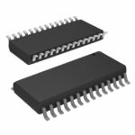 DS92LV1212TMSAX
The activity of extra discounts on wholesale prices is in full swing…
Please fill in your contact information and we will send you the latest wholesale price list.





