 ChipApex | Global Electronic Components Supplier
SEARCH
Search Product
Search Post
— IC芯片 | 连接器 | 传感器 | 被动器件 —
Search productSearch post
— IC芯片 | 连接器 | 传感器 | 被动器件 —
Consult the customer manager about the wholesale price.
consultation hotline:86-132-6715-2157
email:[email protected]
Contact the product manager for consultation. One-stop consultation is available.
Do you want a lower wholesale price? Please send us your inquiry and we will reply immediately.
The DSC557-0343FI0 is a two-output PCI Express clock generator from the DSC557-03 series, manufactured by Microchip Technology. It utilizes silicon MEMS technology to provide a 100 MHz differential output without requiring an external 25 MHz crystal. The device supports PCIe Gen1 through Gen4 specifications and features HCSL and LVDS output formats. It operates within a supply voltage range of 2.25V to 3.6V and is rated for an industrial temperature range of -40°C to +85°C. The component is housed in a space-saving 14-VFQFN package (2.5x3.2 mm) with an exposed pad.
Verify the specific ordering suffix 'I' confirms the -40°C to +85°C industrial temperature rating and 'FI0' indicates the 14-QFN package with HCSL/LVDS outputs. Confirm the manufacturing lot date code against project requirements. Ensure ESD precautions are taken during handling as the device is sensitive to electrostatic discharge. Check for any recent Product Change Notifications regarding packaging or marking updates.
Select this model when a dual-output PCIe clock generator is required for Gen1 to Gen4 interfaces. The DSC557-0343FI0 is suitable for designs needing HCSL and LVDS outputs simultaneously. Consider the 14-VFQFN footprint if board space is limited. Verify that the 100 ppm frequency stability meets system jitter requirements. Ensure the power supply voltage remains within the 2.25V to 3.6V range for proper operation.
This component belongs to the DSC557-03 family of two-output PCIe clock generators. It serves as a direct replacement for legacy crystal-based solutions like the ICS557-03. The device leverages MEMS technology to improve reliability and reduce sensitivity to mechanical stress compared to traditional quartz oscillators. It is part of Microchip's broader portfolio of timing solutions for high-speed serial communication standards.
The datasheet identifies the ICS557-03 as a compatible legacy device for direct replacement. When substituting, verify that the target application can accommodate the removal of the external 25 MHz crystal and associated load capacitors. Ensure the new design supports the 14-VFQFN pinout and thermal pad connection requirements specified in the datasheet.
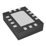 DSC557-0343FI0
The activity of extra discounts on wholesale prices is in full swing…
Please fill in your contact information and we will send you the latest wholesale price list.





