ChipApex | Global Electronic Components Supplier
SEARCH
Search Product
Search Post
— IC芯片 | 连接器 | 传感器 | 被动器件 —
Search productSearch post
— IC芯片 | 连接器 | 传感器 | 被动器件 —
Consult the customer manager about the wholesale price.
consultation hotline:86-132-6715-2157
email:[email protected]
Contact the product manager for consultation. One-stop consultation is available.
Do you want a lower wholesale price? Please send us your inquiry and we will reply immediately.
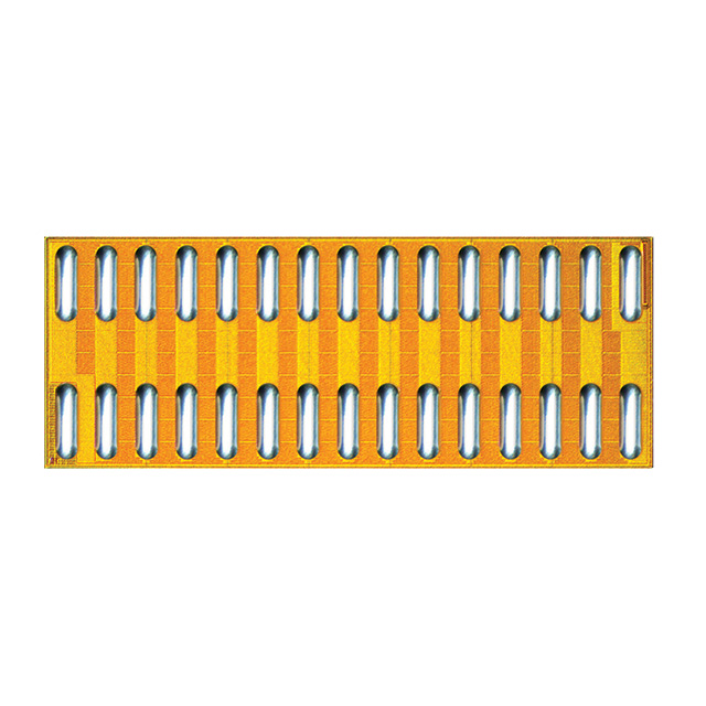
The EPC2021 is an enhancement mode gallium nitride (GaN) power transistor designed for high-efficiency power conversion. It features a drain-source voltage rating of 80 V and a maximum pulsed drain current of 390 A, with a continuous drain current of 90 A at ambient temperature. The device exhibits a low on-resistance of 2.2 mΩ, contributing to reduced conduction losses. Operating within a junction temperature range of -40°C to 150°C, it is supplied as a passivated die with solder bumps in a surface-mount configuration.
Verify the specific revision level and lot traceability upon order confirmation. Confirm that the receiving facility has appropriate electrostatic discharge protection protocols, as the component is supplied as a bare die. Ensure compatibility with the intended substrate or carrier board for proper thermal management and electrical connection via the solder bump interconnects.
Select this component when designing circuits requiring high power density and minimal switching losses. The 80 V rating suits applications operating below this threshold with adequate safety margins. Consider the thermal resistance characteristics of the mounting solution, as heat dissipation relies on direct attachment to a heat sink or PCB copper plane due to the die package format.
This part belongs to the EPC enhancement mode GaN FET family, which replaces traditional silicon MOSFETs in many power stages. Unlike packaged transistors, this specific model is provided as a bare die, requiring integration into custom assemblies or specialized carriers. It shares architectural similarities with other EPC GaN devices but is distinct in its specific voltage and current ratings.
No direct pin-compatible replacements are documented for this bare die configuration. Designers must evaluate alternative GaN dies from the same manufacturer or other vendors based on matching VDS, RDS(on), and package footprint requirements.
 EPC2021
The activity of extra discounts on wholesale prices is in full swing…
Please fill in your contact information and we will send you the latest wholesale price list.