 ChipApex | Global Electronic Components Supplier
SEARCH
Search Product
Search Post
— IC芯片 | 连接器 | 传感器 | 被动器件 —
Search productSearch post
— IC芯片 | 连接器 | 传感器 | 被动器件 —
Consult the customer manager about the wholesale price.
consultation hotline:86-132-6715-2157
email:[email protected]
Contact the product manager for consultation. One-stop consultation is available.
Do you want a lower wholesale price? Please send us your inquiry and we will reply immediately.
The FCB199N65S3 is a single N-channel enhancement mode MOSFET from the SuperFET III series, manufactured by onsemi. It utilizes silicon technology and features a D2PAK-3 (TO-263-3) surface-mount package. Key electrical parameters include a drain-source breakdown voltage of 650 V, a continuous drain current of 14 A, and a maximum gate-source voltage of ±30 V. The device exhibits a typical on-resistance of 170 mΩ at 25°C and a gate charge of 30 nC. It operates within a temperature range of -55°C to +150°C with a power dissipation rating of 98 W.
Verify the specific datasheet revision and RoHS compliance status directly with onsemi or authorized distributors before integration. Confirm that the D2PAK-3 footprint matches the target PCB design. Ensure thermal management solutions align with the 98 W power dissipation rating under expected operating conditions. Cross-reference the part number against any recent obsolescence notices or alternate package options.
Select this component when designing circuits requiring high-voltage handling with moderate current capacity. The 170 mΩ on-resistance offers a balance between conduction loss and cost for medium-power applications. Consider the 14 A current rating relative to thermal constraints and ambient temperatures. The SuperFET III architecture is suitable for designs prioritizing reduced electromagnetic interference due to controlled switching characteristics.
This device belongs to the SuperFET III family, which employs charge-balanced superjunction technology. This architecture allows for lower specific on-resistance compared to conventional planar MOSFETs. The series is engineered to provide superior switching performance while maintaining robust reliability standards for industrial and commercial power electronics.
Direct substitutes within the same series include FCH029N65S3 and NTB190N65S3HF. Verify pinout compatibility and thermal resistance values when considering these alternatives. Ensure that any replacement maintains the required 650 V blocking voltage and meets the specific current and resistance specifications of the original design.
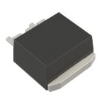 FCB199N65S3
The activity of extra discounts on wholesale prices is in full swing…
Please fill in your contact information and we will send you the latest wholesale price list.





