ChipApex | Global Electronic Components Supplier

SEARCH
Search Product
Search Post
— IC芯片 | 连接器 | 传感器 | 被动器件 —
Search productSearch post
— IC芯片 | 连接器 | 传感器 | 被动器件 —
Consult the customer manager about the wholesale price.
consultation hotline:86-132-6715-2157
email:[email protected]
Contact the product manager for consultation. One-stop consultation is available.
Do you want a lower wholesale price? Please send us your inquiry and we will reply immediately.
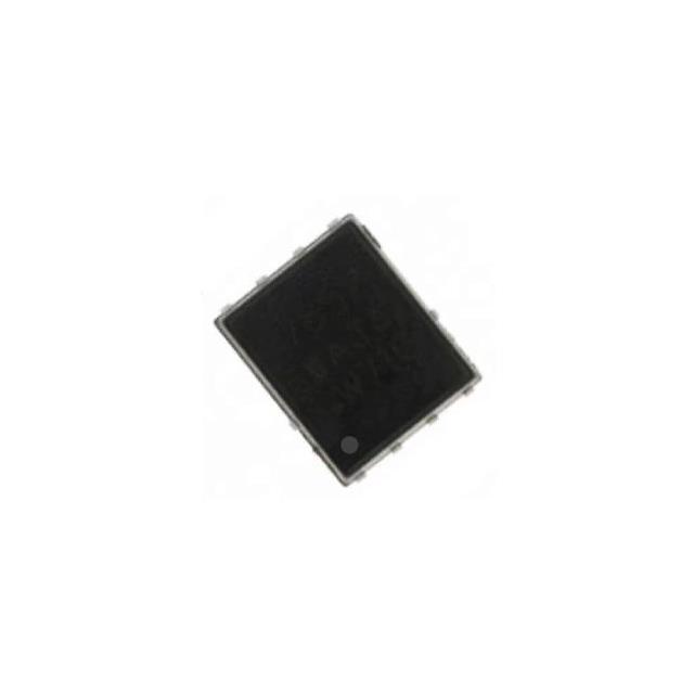
GSFP34010 is listed in the FET, MOSFET Arrays range at ChipApex. The manufacturer field lists Good-Ark Semiconductor. Its product description is MOSFET 2N-CH 100V 20A 8PPAK. Review the specifications below when checking this part for your BOM.
The GSFP34010 is a 100V N-Channel MOSFET manufactured by Good-Ark Semiconductor. It features a maximum drain-source voltage of 100V and a continuous drain current of 20A at 25°C case temperature. The device exhibits a typical on-resistance of 26mΩ and a maximum of 34mΩ at VGS=10V and ID=10A. Key electrical parameters include a gate threshold voltage range of 1.1V to 2.8V, total gate charge of 16nC, and reverse recovery time of 34ns. Power dissipation reaches 19W at 25°C with a junction-to-case thermal resistance of 6.58°C/W.
Verify the specific package marking and date code against the manufacturer's latest documentation before integration. Confirm that the thermal design accounts for the specified junction-to-case resistance under actual operating conditions. Ensure the gate drive voltage aligns with the absolute maximum ratings to prevent dielectric breakdown.
Select this component when a 100V rating and 20A continuous current capability are required in a compact surface mount form factor. Consider the 34mΩ on-resistance limit for conduction loss calculations. Evaluate the thermal environment to ensure the 19W dissipation rating remains within safe operating limits during steady-state operation.
This part belongs to the Good-Ark Semiconductor discrete semiconductor portfolio, specifically within their N-Channel MOSFET category. The device is designed using modern planar trench technology to balance conduction losses and switching speeds. It serves as a solid-state switch alternative to mechanical relays or bipolar transistors in low-voltage DC applications.
Cross-reference pinout compatibility and thermal resistance values when substituting. Verify that any alternative device meets the 100V drain-source voltage requirement and maintains similar gate charge characteristics for equivalent switching performance.
The maximum pulsed drain current is 80A at a case temperature of 25°C.
The on-resistance increases as the junction temperature rises, following the normalized curve provided in the datasheet specifications.
The reverse recovery charge is typically 37nC under test conditions of IS=10A, VGS=0V, VR=50V, and dIF/dt=100A/us.
Explore related parts through FETs, MOSFETs, Transistors, Discrete Semiconductor Products, all product categories.
 GSFP34010

The activity of extra discounts on wholesale prices is in full swing…
Please fill in your contact information and we will send you the latest wholesale price list.