 ChipApex | Global Electronic Components Supplier
SEARCH
Search Product
Search Post
— IC芯片 | 连接器 | 传感器 | 被动器件 —
Search productSearch post
— IC芯片 | 连接器 | 传感器 | 被动器件 —
Consult the customer manager about the wholesale price.
consultation hotline:86-132-6715-2157
email:[email protected]
Contact the product manager for consultation. One-stop consultation is available.
Do you want a lower wholesale price? Please send us your inquiry and we will reply immediately.
The HMC573LC3B is a x2 active broadband frequency multiplier utilizing GaAs PHEMT technology in a leadless RoHS compliant SMT package. It operates with an output frequency range of 8 to 22 GHz. The device requires a maximum supply voltage of 5.5 V and a minimum of 4.5 V, drawing a typical operating current of 92 mA. Power dissipation is rated at 719 mW. It is housed in a QFN-12 (3x3 mm) package and functions within a temperature range of -40 C to +85 C.
Verify the specific suffix LC3B against the official Analog Devices datasheet to confirm pinout and electrical specifications. Ensure compatibility with the intended PCB footprint, as the component uses a 12-VFQFN package. Confirm that the design supports the required 5V supply rail and thermal management for 719 mW dissipation. Check for moisture sensitivity level requirements during assembly processing.
Select this component when a wide bandwidth multiplication factor is required from 8 GHz to 22 GHz. It is suitable for designs needing low phase noise performance typical of GaAs PHEMT technology. Consider the 3x3 mm package size for space-constrained applications. Ensure the input drive level matches the datasheet recommendations for optimal output power.
The HMC573LC3B belongs to the HMC573 series of RF multipliers manufactured by Analog Devices Inc. These components are designed for wireless infrastructure and satellite communications. The series leverages advanced GaAs processes to deliver reliable performance in demanding RF environments. This specific part number denotes the commercial grade variant in the standard SMT package.
Check Analog Devices documentation for direct cross-references or updated revisions within the HMC573 family. Verify if alternative packages or suffixes offer identical electrical characteristics. Ensure any substitute maintains the same 12-pin QFN footprint and thermal properties.
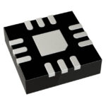 HMC573LC3B
The activity of extra discounts on wholesale prices is in full swing…
Please fill in your contact information and we will send you the latest wholesale price list.





