ChipApex | Global Electronic Components Supplier
SEARCH
Search Product
Search Post
— IC芯片 | 连接器 | 传感器 | 被动器件 —
Search productSearch post
— IC芯片 | 连接器 | 传感器 | 被动器件 —
Consult the customer manager about the wholesale price.
consultation hotline:86-132-6715-2157
email:[email protected]
Contact the product manager for consultation. One-stop consultation is available.
Do you want a lower wholesale price? Please send us your inquiry and we will reply immediately.
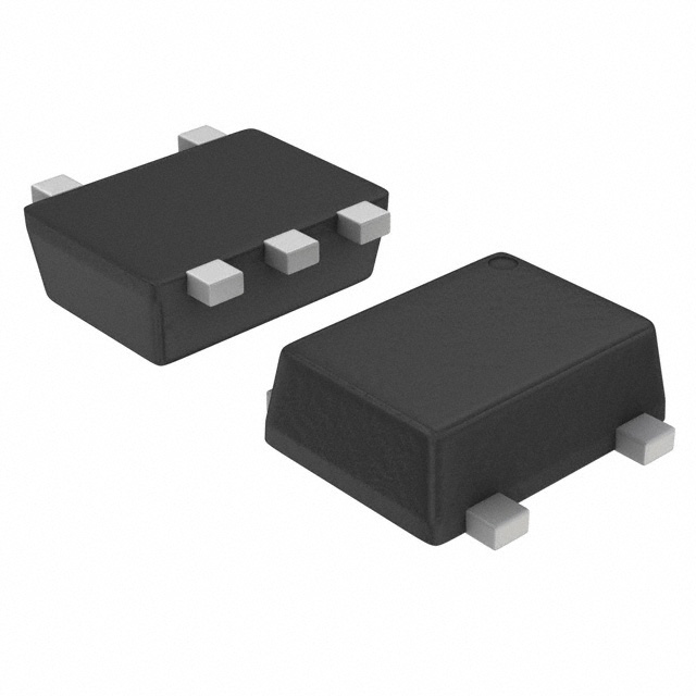
The HN4B01JE(TE85L,F) is a dual bipolar junction transistor (BJT) from Toshiba Semiconductor and Storage, integrating an NPN Q1 and a PNP Q2 in a single SMD package. The device features a maximum collector-emitter voltage of 50V for both transistors and a continuous collector current rating of 150mA. It offers a DC current gain (hFE) range of 120 to 400 at a collector current of 2mA. The transition frequency (fT) is specified at 80MHz under standard test conditions. Total power dissipation is limited to 100mW, with a maximum junction temperature of 150°C.
Verify the component against the official Toshiba datasheet specifications before integration. Confirm that the application design adheres to the absolute maximum ratings, specifically the total power dissipation limit of 100mW. Ensure compliance with environmental directives such as RoHS and avoid usage in unintended high-reliability or safety-critical systems without explicit manufacturer approval.
Select this component for designs requiring matched NPN/PNP pairs within a compact footprint. The ±50V voltage rating suits low-voltage logic interfacing and audio signal processing. Verify thermal management capabilities to maintain the junction temperature below 150°C, considering the 100mW total power dissipation constraint across both transistors.
This part belongs to the HN4B series of dual transistors manufactured using Toshiba's PCT process technology. It integrates complementary silicon epitaxial transistors into a single surface-mount package, facilitating space-constrained circuit layouts while maintaining consistent electrical characteristics between the NPN and PNP elements.
Direct substitutes include other dual BJT packages with matching pinouts and similar electrical parameters. Potential alternatives should be evaluated based on their specific hFE ranges, saturation voltages, and transition frequencies to ensure functional compatibility in existing amplifier topologies.
The device exhibits excellent hFE linearity, with a typical ratio of hFE at 0.1mA to hFE at 2mA of 0.95 for both the NPN and PNP transistors.
The absolute maximum collector-base voltage (VCBO) is rated at 60V for the NPN transistor (Q1) and -50V for the PNP transistor (Q2).
The total collector power dissipation (PC*) is rated at 100mW. This value represents the combined heat dissipation capacity for both the NPN and PNP transistors operating simultaneously within the same package.
 HN4B01JE(TE85L,F)
The activity of extra discounts on wholesale prices is in full swing…
Please fill in your contact information and we will send you the latest wholesale price list.