ChipApex | Global Electronic Components Supplier

SEARCH
Search Product
Search Post
— IC芯片 | 连接器 | 传感器 | 被动器件 —
Search productSearch post
— IC芯片 | 连接器 | 传感器 | 被动器件 —
Consult the customer manager about the wholesale price.
consultation hotline:86-132-6715-2157
email:[email protected]
Contact the product manager for consultation. One-stop consultation is available.
Do you want a lower wholesale price? Please send us your inquiry and we will reply immediately.
The ICL7621BCSA+ is a dual-channel monolithic CMOS operational amplifier from the ICL761X–ICL764X family. It features an input offset voltage (VOS) of 5mV maximum at +25°C and operates within a supply voltage range of ±1V to ±8V, or single supplies from 2V to 16V. The device provides pin-selectable quiescent currents of 10μA, 100μA, or 1000μA per amplifier in compatible variants, though this specific part has fixed settings. It exhibits ultra-low bias current of 1pA typical and offers rail-to-rail output swing capability.
Verify the component status as discontinued on manufacturer databases before finalizing designs. Confirm that the 'SA' suffix corresponds to the 8-pin Slim Small Outline package and that the 'C' temperature grade meets the required operating range of 0°C to +70°C. Ensure compatibility with existing PCB footprints due to industry-standard pinouts.
Select this component when extremely low input bias current is critical for high-impedance signal sources. The dual configuration allows for cost-effective implementation of differential stages. Consider the trade-off between bandwidth and power consumption if variable quiescent current control is needed, as this specific variant may have fixed internal settings compared to single-channel counterparts.
This device belongs to the ICL76XX series of precision CMOS amplifiers known for their high input impedance and low power consumption. The 'B' designation indicates a specific input offset voltage grade, while 'SA' denotes the surface-mount plastic package. It serves as a drop-in replacement for legacy bipolar op-amps in applications requiring minimal input current draw.
Check for direct pin-compatible alternatives within the same ICL76XX family. Verify that substitute parts maintain the required input bias current specifications and supply voltage ranges. Ensure that any replacement supports the necessary temperature operating conditions.
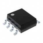 ICL7621BCSA+

The activity of extra discounts on wholesale prices is in full swing…
Please fill in your contact information and we will send you the latest wholesale price list.