 ChipApex | Global Electronic Components Supplier
SEARCH
Search Product
Search Post
— IC芯片 | 连接器 | 传感器 | 被动器件 —
Search productSearch post
— IC芯片 | 连接器 | 传感器 | 被动器件 —
Consult the customer manager about the wholesale price.
consultation hotline:86-132-6715-2157
email:[email protected]
Contact the product manager for consultation. One-stop consultation is available.
Do you want a lower wholesale price? Please send us your inquiry and we will reply immediately.
The Renesas ICS95V2F857AGLF is a single-circuit DDR clock buffer and driver designed for memory applications. It features a zero-delay buffering architecture with an integrated PLL, supporting a maximum frequency of 233MHz. The device accepts LVCMOS input and provides SSTL-2 outputs in a 1:10 ratio. It operates on a supply voltage range of 2.3V to 2.7V within an ambient temperature range of 0°C to 85°C. The component is housed in a 48-TFSOP surface-mount package.
Verify the specific ordering suffix against the manufacturer's official datasheet to confirm pinout compatibility and electrical specifications. Ensure the selected variant matches the required operating temperature range and voltage supply constraints for the target design environment.
Select this component when designing DDR memory interfaces requiring precise clock skew management. Confirm that the system power supply remains within the 2.3V to 2.7V range. Verify that the 48-TFSOP package dimensions fit the PCB layout constraints and that the thermal requirements are met for the intended operating temperature range.
This part belongs to the Renesas clock timing portfolio, specifically engineered for application-specific clock distribution. It serves as a critical interface between system clocks and high-speed memory modules, ensuring signal integrity and timing accuracy in complex digital systems.
Consult the manufacturer's obsolescence notices or cross-reference tools for verified substitute part numbers. Ensure any replacement maintains identical pinout, voltage levels, and performance characteristics to avoid redesign efforts.
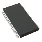 ICS95V2F857AGLF
The activity of extra discounts on wholesale prices is in full swing…
Please fill in your contact information and we will send you the latest wholesale price list.





