 ChipApex | Global Electronic Components Supplier
SEARCH
Search Product
Search Post
— IC芯片 | 连接器 | 传感器 | 被动器件 —
Search productSearch post
— IC芯片 | 连接器 | 传感器 | 被动器件 —
Consult the customer manager about the wholesale price.
consultation hotline:86-132-6715-2157
email:[email protected]
Contact the product manager for consultation. One-stop consultation is available.
Do you want a lower wholesale price? Please send us your inquiry and we will reply immediately.
The ICS9P946AFLF is a clock buffer integrated circuit manufactured by Renesas Electronics Corporation, designed for memory and DDR/DDR2 applications. It features two circuits with a 1:06 input-to-output ratio and supports differential input/output signals. The device operates at a maximum frequency of 533 MHz with a 3.3V supply voltage. It is housed in a 48-BSSOP package (7.50mm width) and functions within an operating temperature range of 0°C to 70°C.
Verify the specific package variant and lead times with authorized distributors, as availability may vary. Confirm RoHS compliance status through official documentation before procurement. Ensure the 48-SSOP footprint matches the target PCB design requirements.
Select this component for designs requiring low-jitter clock distribution to multiple DDR or DDR2 memory modules. Ensure the system environment stays within the 0°C to 70°C operating range. Verify that the 3.3V supply rail is stable and meets the noise specifications outlined in the datasheet.
This part belongs to the Application Specific Clock/Timing category from Renesas Electronics. It serves as a specialized buffer for high-speed memory interfaces, distinct from general-purpose clock generators or oscillators.
Check for direct pin-compatible alternatives within the Renesas portfolio that support similar DDR frequencies. Verify if newer generations offer improved jitter performance or extended temperature ranges while maintaining the 48-SSOP package.
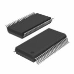 ICS9P946AFLF
The activity of extra discounts on wholesale prices is in full swing…
Please fill in your contact information and we will send you the latest wholesale price list.






